In light load, if output voltage decreases, the trans wire
wound voltage in primary part also decreases proportionately
and the Vin terminal voltage in primary part reaches lower
than operation stop volate so that OCP circuit stops operat-
ing. In this case, the circuit current decreases so that the Vin
terminal voltage increases in proportion to charge current by
start resistance Rs again and intermittent operation occurres
which restarts in operation start voltage.
The advantage of adding the Protection circut against over-
current is as follows. When input voltage is high, the surge
voltage becomes low by controlling MOSFET drain current
low and stress of voltage in MOSFET becomes less in start
and overload.
And stress of current in secondary Diode can be also less by
controlling output voltage regular.
(4) Latch circuit
Latch circuit is to stop power circuit operating by keeping the
output of oscillator low in operating of two circuits (OVP &
TSD) which protect Over-voltage and overheat.
Latch circuit is to protect malfunction caused by noise etc..
And this circuit starts to function when OVP and TSD oper-
ates for more than 8 seconds. In this case, delay time is set
by timer circuit in control IC.
Though Latch circuit operates, Constant voltage power (Reg)
circuit in control IC is also operating and the circuit current is
high. So the Vin terminal voltage decreases rapidly.
If the Vin terminal voltage becomes lower than operation stop
voltage 10V (TYP), circuit current becomes below 400uA and
the Vin terminal voltage begins to increase. On the contrary, if
the Vin terminal voltage reaches operation start voltage 16V
(TYP), circuit current begins to increase and the Vin terminal
voltage begins to decrease.
In other words, the Vin terminal voltage rises and falls
between 10V (TYP) and 16V (TYP).
Like this, the latch circuit protects the Vin terminal voltage
from increasing abnormally.
Releasing latch circuit is done by making the Vin terminal
voltage lower than 6.5V and generally latch circuit is restarted
after cutting AC input.
(5) Protect circuit against overheat
This circuit lets latch circuit operate when the frame tempera-
ture of Hybrid IC is above 140°C(Min).
Actual temperature is detected by control circuit element. This
is to protect MOSFET from overheat which is caused by the
system that MOSFET and control circuit element are on the
same frame.
(6) Protect circuit against over-voltage
This circuit lets latch circuit operate when the Vin terminal
voltage exceeds 22.5V (TYP) and this is used to protect the
Vin terminal in control circuit from over-voltage.
Commonly the Vin terminal is supplied with subsidiary wire
wound of Trans and this voltage is in proportion to output
voltage so that this Protect circuit against over-voltage oper-
ates in over-voltage output in secondary part when the circuit
of detecing voltage is open.
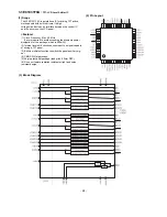
1.5 STR G6153T(ST-BY STR)
(1) Description of each terminals
Others
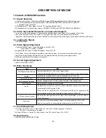
(2) Operation stop circuit (UVLO)
This begins operation control if voltage is supplied to low sub-
sidiary current terminal (Vcc) 5PIN.
If the supplied voltage in the same terminal reaches operation
start current voltage (Vcc), 17.5V (TYP), current is supplied to
circuits within IC and then the operation stop circuit (UVLO)
begins operaiton control and high impedence is sustained
until the supplied voltage reaches the same voltage. In this
time, the supplied current is circuit current (Icc) in not operat-
ing and it is 70Ua (Max).
If the operation stop circuit begins operation control, circuit
current (Icc) in operation, about 15mA flows in the same ter-
minal. In controlling operation, if the supplied voltage in this
terminal goes below operation stop current voltage (Vcc),
11.5V (TYP), IC stops functioning.
Like this, this terminal plays a roll to detect supplied voltage
and to control operation start in low voltage input.
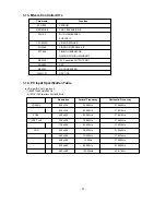
(3) Internal Oscillator (OSC)
Condernsor to determine oscillation frequency : Ct
If IC begins operating, Ct is charged from internal power by
constant current I1. At this moment, both SW1 and SW2
become open.
If electric potential of charge reaches about 4V, comparator
reverses, and SW1 and SW2 are on simultaneously.
If setting the state that I1 is lower than I2, SW1 becomes on,
Ct gets discharged and Vt decreases.
Oscillation is made by these operations.
Maximum Duty cycle of oscillator is set to 80% (TYP) and fre-
quency is set to 100KHz (TYP). Globular shaped wave output
of Comparator is used as timing clock in internal circuit and
triangle shaped wave output is used as standard signal for
transforming pulse width which will be mentioned later.
- 18 -
1
2
3
4
5
D
OCP
GND
FB
Vcc
No.
Symbol
Name
Function
MOSFET drain
Drain
terminal
Input signal of detecting
over-current in primary
part
Over-current
terminal
Ground
Ground
terminal
Input signal of controlling
constant voltage
Feed-Back
terminal
Input control circuit power
Power
terminal
Symbol Function
OVP
Protect circuit against over-voltage
OLP
Protect circuit against overload
TSD Protect circuit against overheat
SS Soft start function


