

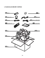
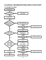
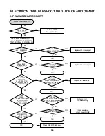


1-4
ESD PRECAUTIONS
Electrostatically Sensitive Devices (ESD)
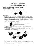
Some semiconductor (solid state) devices can be damaged easily by static electricity. Such components
commonly are called electrostatically sensitive devices (ESD). Examples of typical ESD devices are
integrated circuits and some field-effect transistors and semiconductor chip components. The following
techniques should be used to help reduce the incidence of component damage caused by static electricity.
1. Immediately before handling any semiconductor component or semiconductor-equipped assembly, drain
off any electrostatic charge on your body by touching a know earth ground. Alternatively, obtain and
wear a commercially available discharging wrist strap device, which should be removed for potential
shock reasons prior to applying power to the unit under test.
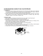
2. After removing an electrical assembly equipped with ESD devices, place the assembly on a conductive
surface such as aluminum foil, to prevent electrostatic charge buildup or exposure of the assembly.
3. Use only a grounded-tip soldering iron to solder or unsolder ESD devices.
4. Use only an anti-static solder removal device. Some solder removal devices not classified as "anti-static"
can generate electrical charges sufficient to damage ESD devices.
5. Do not use freon-propelled chemicals These can generate electrical charges sufficient to damage ESD
devices.
6. Do not remove a replacement ESD device from its protective package until immediately before you are
ready to install it. (Most replacement ESD devices are packaged with leads electrically shorted together
by conductive foam, aluminum foil or comparable conductive materials).
7. Immediately before removing the protective material from the leads of a replacement ESD device, touch
the protective material to the chassis or circuit assembly into which the device will by installed.
CAUTION : BE SURE NO POWER IS APPLIED TO THE CHASSIS OR CIRCUIT, AND OBSERVE ALL
OTHER SAFETY PRECAUTIONS.
8. Minimize bodily motions when handing unpackaged replacement ESD devices. (Otherwise harmless
motion such as the brushing together of your clothes fabric or the lifting of your foot from a carpeted floor
can generate static electricity sufficient to damage an ESD device).
[CAUTION. GRAPHIC SYMBOLS]
THE LIGHTNING FLASH WITH ARROWHEAD SYMBOL. WITHIN AN EQUILATERAL
TRIANGLE, IS INTENDED TO ALERT THE SERVICE PERSONNEL TO THE PRESENCE
OF UNINSULATED "DANGEROUS VOLTAGE" THAT MAY BE OF SUFFICIENT
MAGNITUDE TO CONSTITUTE A RISK OF ELECTRIC SHOCK.
THE EXCLAMATION POINT WITHIN AN EQUILATERAL TRIANGLE IS INTENED TO
ALERT THE SERVICE PERSONNEL TO THE PRESENCE OF IMPORTANT SAFETY
INFORMATION IN SERVICE LITERATURE.
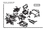
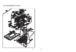
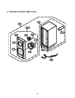
Summary of Contents for MBD-D102X
Page 7: ...1 6 MEMO ...
Page 10: ...2 5 3 SPEAKER SECTION MBS D102V 750 751 752 754 755 757 A70A 758 A70 757A 759 756 753 ...
Page 35: ...3 24 4 FOCUS WAVEFORM 1 FDO 2 F 3 F INSERT CD INSERT DVD 1 FDO 2 F 3 F ...
Page 37: ...3 26 7 TRACKING SIGNAL 1 Tro 2 Tr 3 Tr 8 RF WAVEFORM ...
Page 38: ...3 27 9 DISK TYPE JUGEMENT WAVEFORM 1 F 2 FDO 3 SVRRF DVD CD ...
Page 50: ...3 39 7 MC4580 7 1 PIN CONFIGURATION 7 2 TEST CIRCUIT 7 3 ABSOLUTE MAXIMUM RATINGS TA 25 ...
Page 60: ...3 49 3 50 WIRING DIAGRAM ...
Page 62: ...3 53 3 54 2 MAIN FRONT BLOCK DIAGRAM ...
Page 64: ...3 57 3 58 2 MAIN INTERFACE PWM SCHEMATIC DIAGRAM ...
Page 65: ...3 59 3 60 3 MPEG SCHEMATIC DIAGRAM ...
Page 66: ...3 61 3 62 4 SERVO SCHEMATIC DIAGRAM ...
Page 67: ...3 63 3 64 5 INTERFACE SCHEMATIC DIAGRAM ...
Page 68: ...3 65 3 66 6 FRONT SCHEMATIC DIAGRAM ...
Page 69: ...3 67 3 68 7 FRONT MIC SCHEMATIC DIAGRAM ...
Page 70: ...3 69 3 70 8 IPOD 1 SCHEMATIC DIAGRAM OPTION ...
Page 71: ...3 71 3 72 9 IPOD 2 SCHEMATIC DIAGRAM OPTION ...
Page 72: ...3 73 3 74 10 2 CHANNEL AMP SCHEMATIC DIAGRAM ...
Page 73: ...3 75 3 76 11 BLUTHOOTH MODULE SCHEMATIC DIAGRAM OPTION ...
Page 75: ...3 79 3 80 1 MAIN P C BOARD TOP VIEW PRINTED CIRCUIT BOARD DIAGRAMS ...
Page 76: ...3 81 3 82 MAIN P C BOARD BOTTOM VIEW ...
Page 77: ...3 83 3 84 2 FRONT P C BOARD TOP VIEW BOTTOM VIEW ...
Page 78: ...3 85 3 86 3 SMPS P C BOARD TOP VIEW BOTTOM VIEW ...