


- 1-4 -
❏
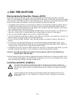
ESD PRECAUTIONS
Electrostatically Sensitive Devices (ESD)
Some semiconductor (solid state) devices can be damaged easily by static electricity. Such components
commonly are called Electrostatically Sensitive Devices (ESD). Examples of typical ESD devices are integrated
circuits and some field-effect transistors and semiconductor chip components. The following techniques should
be used to help reduce the incidence of component damage caused by static electricity.
1. Immediately before handling any semiconductor component or semiconductor-equipped assembly, drain off
any electrostatic charge on your body by touching a known earth ground. Alternatively, obtain and wear a
commercially available discharging wrist strap device, which should be removed for potential shock reasons
prior to applying power to the unit under test.
2. After removing an electrical assembly equipped with ESD devices, place the assembly on a conductive sur-
face such as aluminum foil, to prevent electrostatic charge buildup or exposure of the assembly.
3. Use only a grounded-tip soldering iron to solder or unsolder ESD devices.
4. Use only an anti-static solder removal device. Some solder removal devices not classified as "anti-static" can
generate electrical charges sufficient to damage ESD devices.
5. Do not use freon-propelled chemicals. These can generate electrical charges sufficient to damage ESD
devices.
6. Do not remove a replacement ESD device from its protective package until immediately before you are
ready to install it. (Most replacement ESD devices are packaged with leads electrically shorted together by
conductive foam, aluminum foil or comparable conductive materials).
7. Immediately before removing the protective material from the leads of a replacement ESD device, touch the
protective material to the chassis or circuit assembly into which the device will by installed.
CAUTION : BE SURE NO POWER IS APPLIED TO THE CHASSIS OR CIRCUIT, AND OBSERVE ALL
OTHER SAFETY PRECAUTIONS.
8. Minimize bodily motions when handing unpackaged replacement ESD devices. (Otherwise harmless motion
such as the brushing together of your clothes fabric or the lifting of your foot from a carpeted floor can gen-
erate static electricity sufficient to damage an ESD device).
CAUTION. GRAPHIC SYMBOLS
THE LIGHTNING FLASH WITH APROWHEAD SYMBOL. WITHIN AN EQUILATERAL TRIANGLE, IS
INTENDED TO ALERT THE SERVICE PERSONNEL TO THE PRESENCE OF UNINSULATED “DANGER-
OUS VOLTAGE” THAT MAY BE OF SUFFICIENT MAGNITUDE TO CONSTITUTE A RISK OF ELECTRIC
SHOCK.
THE EXCLAMATION POINT WITHIN AN EQUILATERAL TRIANGLE IS INTENDED TO ALERT THE
SERVICE PERSONNEL TO THE PRESENCE OF IMPORTANT SAFETY INFORMATION IN SERVICE
LITERATURE.
Summary of Contents for LH-D6240A
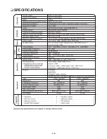
Page 5: ... 1 5 SPECIFICATIONS ...
Page 6: ... 1 6 LOCATION OF CUSTOMER CONTROLS FRONT PANEL DISPLAY WINDOW ...
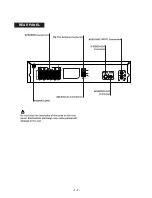
Page 7: ... 1 7 REAR PANEL ...
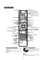
Page 8: ... 1 8 Remote Control ...
Page 9: ... 2 1 SECTION 2 AUDIO PART AUDIO TROUBLESHOOTING GUIDE 1 POWER SUPPUY CIRCUIT ...
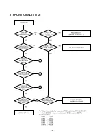
Page 10: ... 2 2 2 FRONT CIRCUIT 1 2 ...
Page 11: ... 2 3 3 FRONT CIRCUIT 2 2 ...
Page 12: ... 2 4 MEMO ...
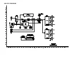
Page 13: ... BLOCK DIAGRAM 2 5 2 6 ...
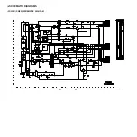
Page 14: ...2 7 2 8 SCHEMATIC DIAGRAMS POWER SMPS SCHEMATIC DIAGRAM ...
Page 15: ...2 9 2 10 µ COM SCHEMATIC DIAGRAM ...
Page 16: ...2 11 2 12 FRONT POWER 2nd SCHEMATIC DIAGRAM ...
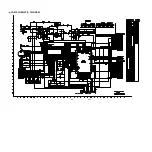
Page 17: ...2 13 2 14 DAP SCHEMATIC DIAGRAM ...
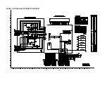
Page 18: ...2 15 2 16 AMP SCHEMATIC DIAGRAM ...
Page 19: ...2 17 2 18 WIRING DIAGRAM ...
Page 20: ...2 19 2 20 PRINTED CIRCUIT BOARD DIAGRAMS MAIN P C BOARD DIAGRAM SOLDER SIDE ...
Page 21: ...2 21 2 22 MAIN P C BOARD DIAGRAM COMPONENT SIDE ...
Page 22: ...2 23 2 24 POWER SMPS P C BOARD SOLDER SIDE ...
Page 23: ...2 25 2 26 FRONT P C BOARD DIAGRAM SOLDER SIDE ...
Page 24: ... 3 1 SECTION 3 DVD PART DVD TROUBLESHOOTING GUIDE 1 Power check flow ...
Page 25: ... 3 2 2 Test debug flow ...
Page 26: ... 3 3 ...
Page 27: ... 3 4 ...
Page 28: ... 3 5 ...
Page 29: ... 3 6 ...
Page 30: ... 3 7 ...
Page 34: ... 3 11 2 Tray close waveform 3 Tray open waveform ...
Page 36: ... 3 13 6 LASER POWER CONTROL RELATED SIGNAL NO DISC CONDITION 7 DISC TYPE JUDGEMENT WAVEFORM ...
Page 37: ... 3 14 ...
Page 38: ... 3 15 8 FOCUS ON WAVEFORM ...
Page 39: ... 3 16 9 SPINDLE CONTROL WAVEFORM NO DISC CONDITION ...
Page 40: ... 3 17 10 TRACKING CONTROL RELATED SIGNAL System checking ...
Page 41: ... 3 18 11 RF WAVEFORM 12 MT1379 AUDIO OPTICAL AND COAXIAL OUTPUT ASPDIF ...
Page 42: ... 3 19 13 MT1379 VIDEO OUTPUT WAVEFORM 1 Full colorbar signal CVBS 2 Y ...
Page 43: ... 3 20 3 C 14 AUDIO OUTPUT FORM AUDIO DAC 1 Audio related Signal ...
Page 44: ...3 21 3 22 DVD PART SCHEMATIC DIAGRAMS MPEG SCHEMATIC DIAGRAM ...
Page 45: ...3 23 3 24 SERVO SCHEMATIC DIAGRAM ...
Page 46: ...3 25 3 26 AUDIO SCHEMATIC DIAGRAM ...
Page 47: ...3 27 3 28 VOLTAGE SHEET IC TR ...
Page 48: ...3 29 3 30 PRINTED CIRCUIT DIAGRAM DVD P C BOARD SOLDER SIDE ...
Page 49: ...3 31 3 32 DVD P C BOARD COMPONENT SIDE ...
Page 51: ...4 3 4 4 DECK MECHANISM EXPLODED VIEW ...
Page 52: ...4 5 4 6 MEMO MEMO ...
Page 53: ... 5 1 SECTION 5 SPEAKER SECTION MODEL LHS D6240W 856 859 859 855 853 861 860 852 851 ...
Page 54: ... 5 2 MODEL LHS D6240T 861 854 853 860 852 851 850 ...


