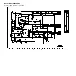
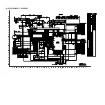
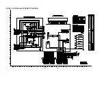
Summary of Contents for LH-D6240A
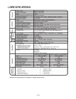
Page 5: ... 1 5 SPECIFICATIONS ...
Page 6: ... 1 6 LOCATION OF CUSTOMER CONTROLS FRONT PANEL DISPLAY WINDOW ...
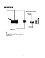
Page 7: ... 1 7 REAR PANEL ...
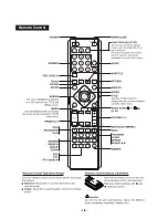
Page 8: ... 1 8 Remote Control ...
Page 9: ... 2 1 SECTION 2 AUDIO PART AUDIO TROUBLESHOOTING GUIDE 1 POWER SUPPUY CIRCUIT ...
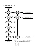
Page 10: ... 2 2 2 FRONT CIRCUIT 1 2 ...
Page 11: ... 2 3 3 FRONT CIRCUIT 2 2 ...
Page 12: ... 2 4 MEMO ...
Page 13: ... BLOCK DIAGRAM 2 5 2 6 ...
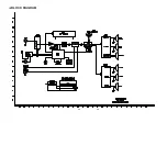
Page 14: ...2 7 2 8 SCHEMATIC DIAGRAMS POWER SMPS SCHEMATIC DIAGRAM ...
Page 15: ...2 9 2 10 µ COM SCHEMATIC DIAGRAM ...
Page 16: ...2 11 2 12 FRONT POWER 2nd SCHEMATIC DIAGRAM ...
Page 17: ...2 13 2 14 DAP SCHEMATIC DIAGRAM ...
Page 18: ...2 15 2 16 AMP SCHEMATIC DIAGRAM ...
Page 19: ...2 17 2 18 WIRING DIAGRAM ...
Page 20: ...2 19 2 20 PRINTED CIRCUIT BOARD DIAGRAMS MAIN P C BOARD DIAGRAM SOLDER SIDE ...
Page 21: ...2 21 2 22 MAIN P C BOARD DIAGRAM COMPONENT SIDE ...
Page 22: ...2 23 2 24 POWER SMPS P C BOARD SOLDER SIDE ...
Page 23: ...2 25 2 26 FRONT P C BOARD DIAGRAM SOLDER SIDE ...
Page 24: ... 3 1 SECTION 3 DVD PART DVD TROUBLESHOOTING GUIDE 1 Power check flow ...
Page 25: ... 3 2 2 Test debug flow ...
Page 26: ... 3 3 ...
Page 27: ... 3 4 ...
Page 28: ... 3 5 ...
Page 29: ... 3 6 ...
Page 30: ... 3 7 ...
Page 34: ... 3 11 2 Tray close waveform 3 Tray open waveform ...
Page 36: ... 3 13 6 LASER POWER CONTROL RELATED SIGNAL NO DISC CONDITION 7 DISC TYPE JUDGEMENT WAVEFORM ...
Page 37: ... 3 14 ...
Page 38: ... 3 15 8 FOCUS ON WAVEFORM ...
Page 39: ... 3 16 9 SPINDLE CONTROL WAVEFORM NO DISC CONDITION ...
Page 40: ... 3 17 10 TRACKING CONTROL RELATED SIGNAL System checking ...
Page 41: ... 3 18 11 RF WAVEFORM 12 MT1379 AUDIO OPTICAL AND COAXIAL OUTPUT ASPDIF ...
Page 42: ... 3 19 13 MT1379 VIDEO OUTPUT WAVEFORM 1 Full colorbar signal CVBS 2 Y ...
Page 43: ... 3 20 3 C 14 AUDIO OUTPUT FORM AUDIO DAC 1 Audio related Signal ...
Page 44: ...3 21 3 22 DVD PART SCHEMATIC DIAGRAMS MPEG SCHEMATIC DIAGRAM ...
Page 45: ...3 23 3 24 SERVO SCHEMATIC DIAGRAM ...
Page 46: ...3 25 3 26 AUDIO SCHEMATIC DIAGRAM ...
Page 47: ...3 27 3 28 VOLTAGE SHEET IC TR ...
Page 48: ...3 29 3 30 PRINTED CIRCUIT DIAGRAM DVD P C BOARD SOLDER SIDE ...
Page 49: ...3 31 3 32 DVD P C BOARD COMPONENT SIDE ...
Page 51: ...4 3 4 4 DECK MECHANISM EXPLODED VIEW ...
Page 52: ...4 5 4 6 MEMO MEMO ...
Page 53: ... 5 1 SECTION 5 SPEAKER SECTION MODEL LHS D6240W 856 859 859 855 853 861 860 852 851 ...
Page 54: ... 5 2 MODEL LHS D6240T 861 854 853 860 852 851 850 ...

