5. DOWNLOAD
- 113 -
LGE Internal Use Only
Copyright © 011 LG Electronics. Inc. All right reserved.
Only for training and service purposes
zG||ziwGtGGGaGG
㜼 OW[P
LG-A30
Page 1: ...Internal Use Only Service Manual LG A230 Date May 2011 Issue 1 0 ...
Page 2: ... 4 2 RXTrouble 58 4 3TXTrouble 64 4 4 Power OnTrouble 70 4 5 ChargingTrouble 73 4 6VibratorTrouble 76 4 7 LCDTrouble 79 4 8 CameraTrouble 83 4 9 Speaker ReceiverTrouble 87 4 10 EarphoneTrouble 90 4 11 MicrophoneTrouble 93 4 12 SIM Card InterfaceTrouble 96 4 13 Micro SD uSD Trouble 99 4 14 BluetoothTrouble 102 4 15 FM RadioTrouble 105 4 16Wireless FM RadioTrouble 107 5 DOWNLOAD 110 6 BLOCK DIAGRAM ...
Page 3: ...facilities accessed through or connected to it The manufacturer will not be responsible for any charges that result from such unauthorized use B Incidence of Harm If a telephone company determines that the equipment provided to customer is faulty and possibly causing harm or interruption in service to the telephone network it should disconnect telephone service until repair can be done A telephone...
Page 4: ...ation Phone may interfere with sensitive laboratory equipment medical equipment etc Interference from unsuppressed engines or electric motors may cause problems H Electrostatic Sensitive Devices ATTENTION Boards which contain Electrostatic Sensitive Device ESD are indicated by the sign Following information is ESD handling Service personnel should ground themselves by using a wrist strap when exch...
Page 5: ...iate Frequency IF International Portable User Identity IPUI Global System for Mobile Communications GSM General Purpose Interface Bus GPIB Gaussian Minimum Shift Keying GMSK Flexible Printed Circuit Board FPCB Electrostatic Discharge ESD Electrical Erasable Programmable Read Only Memory EEPROM Digital Signal Processing DSP dB relative to 1 milli watt dBm Digital Communication System DCS Digital to...
Page 6: ... Transmitter UART Time Division Multiple Access TDMA Time Division Duplex TDD Travel Adapter TA Side Tone Masking Rating STMR Pseudo SRAM PSRAM Static Random Access Memory SRAM Sending Loudness Rating SLR Subscriber Identity Module SIM Surface Acoustic Wave SAW Real Time Clock RTC Root Mean Square RMS Receiving Loudness Rating RLR Radio Frequency RF Public Switched Telephone Network PSTN Phase Loc...
Page 7: ...pprox 3 hours RX Sensitivity GSM EGSM 109dBm DCS 109dBm TX output power GSM EGSM 32 3dBm Level 5 DCS PCS 29 5dBm Level 0 SIM card type 3V 1 8V Display MAIN 1 77 QVGA 160 Ý 128 pixel Status Indicator Send Key End Key Navi Key Up Down Left Right ANT Internal EAR Phone Jack Yes PC Synchronization Yes Speech coding EFR FR HR Data and Fax Yes GPRS compatibility Class 10 Vibrator Yes Loud Speaker Yes Vo...
Page 8: ... Phase Error RMS 5 degrees Peak 20 degrees 3 Frequency Error 0 1 ppm 4 Power Level Level Power Toler Level Power Toler 6 31dBm 3dB 14 15dBm 3dB 7 29dBm 3dB 15 13dBm 3dB 8 27dBm 3dB 16 11dBm 5dB 9 25dBm 3dB 17 9dBm 5dB 10 23dBm 3dB 18 7dBm 5dB 11 21dBm 3dB 19 5dBm 5dB 12 19dBm 3dB GSM850 EGSM 5 33dBm 2dB 13 17dBm 3dB Level Power Toler Level Power Toler 1 28dBm 3dB 9 12dBm 4dB 2 26dBm 3dB 10 10dBm 4...
Page 9: ... 100 0 5 200 30 250 33 400 60 600 1 200 60 1 200 1 800 60 1 800 3 000 63 3 000 6 000 65 6 000 71 GSM850 EGSM Offset from Carrier kHz Max dBc 100 0 5 200 30 250 33 400 60 600 1 200 60 1 200 1 800 60 1 800 3 000 65 3 000 6 000 65 6 000 73 DCS PCS 6 Output RF Spectrum due to switching transient GSM850 EGSM Offset from Carrier kHz Max dBm 400 19 600 21 1 200 21 1 800 24 Item Description Specification ...
Page 10: ...g transient Offset from Carrier kHz Max dBm 400 22 600 24 1 200 24 1 800 27 7 Spurious Emissions Conduction Emission Status 8 Bit Error Ratio GSM850 EGSM BER Class II 2 439 102 dBm DCS PCS BER Class II 2 439 100 dBm 9 RX Level Report Accuracy 3 dB 10 SLR 12 3 dB 11 Sending Response 300 12 1 000 6 2 000 6 3 000 6 Frequency Hz Max dB Min dB 100 200 4 000 3 400 9 0 0 4 4 12 0 0 4 12 RLR 4 3 dB DCS PC...
Page 11: ... 12 0 2 2 14 STMR 17 dB Mean that Adopt a straight line in between 300 Hz and 1 000 Hz to be Max level in the range 15 Stability Margin 6 dB 20 10 0 7 dB to ARL dB Level Ratio dB 35 30 10 30 7 33 3 33 7 31 7 17 5 22 5 25 5 16 Distortion 17 Side Tone Distortion Three stage distortion 10 18 System frequency 13 MHz tolerance 2 5 ppm 19 32 768KHz tolerance 30 ppm 20 Ringer Volume At least 55 dBspl und...
Page 12: ...Indicator SPG Software Power Gauge 24 Low Voltage Warning Blinking Bar 5 in 950mA 1 time standby 10 in 950mA 1 time standby 5 in 950mA 1 time Call 10 in 950mA 1 time Call 25 Forced shut down Voltage 3 35 0 05V 27 Battery Type Lithium Ion Battery Standard Voltage 3 7 V Battery full charge voltage 4 2 V Capacity 950mAh 28 Travel Charger Switching mode charger Input 100 240V 50 60 Hz Output 4 8V 400m...
Page 13: ...LG Electronics Inc All right reserved Only for training and service purposes 3 TECHNICAL BRIEF 3 TECHNICAL BRIEF 3 TECHNICAL BRIEF LJLWDO 0DLQ 3URFHVVRU LJXUH ROG WP DUGZDUH ORFN LDJUDP 3 1 Digital Main Processor Figure 3 1 1 X Gold 215 Hardware Block Diagram ...
Page 14: ...version receiver Tri Quad band possible with external circuitry Fully integrated digital controlled X0 Additional buffer for 2 external system clocks Fully digital RF Synthesizer incl ȭȟ Transmitter 3 1 3 Baseband DSP 156 MHz TeakLite MCU ARM1176 208 MHz MCU RAM 3 00Mbit Memory I F 512 Mbit Modem GPRS class 12 RX TX CS1 CS4 EGPRS class 12 RX MCS1 MCS9 TX MCS1 MCS4 Cipher Units A51 2 3 GEA 1 2 3 Se...
Page 15: ...ss bus 512 Mbit 16 bit data bus 1 8V 2 8V support Flash RAM NAND Type Serial Flash SPI and SPI 4 Parallel Flash Page Burst Mode 16 bit Demultiplexed 16 bit AD multiplexed 16 bit AAD multiplexed iNAND Type e g oneNAND Memory card SD MMC card interface with 1 or 4 data lines 3 1 5 Connectivity 3xUSIF configurable either as SPI or UART I2C I2S Interfaces 1 8V Direct U SIM 1 8 3V USB2 0 up to 480 Mbit...
Page 16: ...icrophone supported Differential microphone inputs 3 1 7 FM Radio Integrated FM radio FM Stereo RDS Receiver Sensitivity 2 ɆV EMF Support for US EU bands Stereo recording 3 1 8 Power Management Direct to Battery Connection LDOs incl capless DC DC step down converter DC DC step up for white LED supply Battery Type Li Polymer Charging control Battery temperature Watchdog protection Start up on flat ...
Page 17: ...Video post processing Scaling Rotation 90 steps Mirroring Overlay with alpha blending Color conversion YUV RGB 2D vector graphics Lines filled rectangles Bit block transfer e g sprites scrolling antialiased bitmapfonts 3 1 10 Camera 2 Mpx YUV parallel interface HW JPEG encoder 39 Mpx sec 39 MHz Pixel Rate 15 fps 2 Mpx full resolution 3 1 11 Video Capabilities Video Decoding MPEG 4 H 263 QCIF 30 fp...
Page 18: ...For advanced features additional off chip power supplies might be necessary Figure 3 2 1 Block Figure of the PMU Modules X GOLD 215 DC DC Step Down Converter for 1 8V SD1 The DC DC converter generates a 1 8 V supply rail This voltage rail is used to supply main parts of the system like the digital core of the chip via LDO LCORE some parts of the mixed signal macro parts of the RF macro and the ext...
Page 19: ...e supply for the USB transceiver output driver and input If no USB interface is required LUSB can be used as general purpose LDO LAUX The LAUX generates VAUX It is a general purpose LDO and can be used for different functions depending on the phone application e g for the display or camera LMMC The LMMC generates VMMC It is a general purpose LDO and can be used e g for memory cards LSIM The LSIM L...
Page 20: ... 20 LGE Internal Use Only Copyright 2011 LG Electronics Inc All right reserved Only for training and service purposes 3 TECHNICAL BRIEF Table 3 2 1 Power supply Domains without RF ...
Page 21: ...ven by the PMU state machine can be seen in Figure18 After enabling the reference HPGB and waiting for the settling time the battery voltage is measured and compared with the power on threshold If the battery voltage is high enough the SD1 DC DC converter and the LCORE LDO are started A timer ensures that the supply voltage will be stable before the DCXO is enabled The DCXO settling time is ensure...
Page 22: ...Use Only Copyright 2011 LG Electronics Inc All right reserved Only for training and service purposes 3 TECHNICAL BRIEF Figure 3 2 1 First Part of the State Machine Running in Different Power Domains than the Second Part ...
Page 23: ...HNICAL BRIEF 23 LGE Internal Use Only Copyright 2011 LG Electronics Inc All right reserved Only for training and service purposes Figure 3 2 2 Second Main Part of the Startup State Machine in the VPMU Domain ...
Page 24: ...uring phone operation also 3 2 4 Switching on due to RTC alarm The real time clock can generate a wakeup signal called RTC alarm This signal is sampled from the state machine and after successfully detecting a high the system is switched on 3 2 5 Switching on due to charging When a battery with a voltage below the SSONLEV level is inserted the state machine will not start the system As long as the...
Page 25: ...ble the charger watchdog for safety 3 2 6 Power Supply Start up sequence In order to avoid an excessive drop on the battery voltage caused by in rush current during system power on possibly leading to system instability and hick ups a staggered turn on approach for the regulators is implemented The regulators are turned on in a well defined sequence thus spreading the in rush current transients ov...
Page 26: ... 26 LGE Internal Use Only Copyright 2011 LG Electronics Inc All right reserved Only for training and service purposes 3 TECHNICAL BRIEF Figure 3 2 3 Start Up Sequence triggered by First Connect Event ...
Page 27: ...nal controls for example the ɆC subsystem and releases reset for the controller During normal start up the PMU releases the reset_pmu_n_o signal after entering the SYSTEM ON state At this time the resetout_o signal is high the RESET_N pad is not pulled low and therefore the reset_postscu_n_o signal follows the reset_pmu_n_o signal That means the ɆC reset will be released and the ɆC starts operatio...
Page 28: ... the PMU enables the DCXO After the system is running the DCXO is controlled by the SCU of the baseband by using the vcxo_enable signal This is handled by a dedicated logic in the PMU see Figure 21 As long as rf_sysclk_en_pmu the output of the PMU state machine is high vcxo_enable controls the rf_sysclk_en signal to the RF If rf_sysclk_en_pmu is low the DXCO is switched off independent from vcxo_e...
Page 29: ...n_o signal That means all PMU register are reset in OFF state For details about the SW reset see chapter External Reset Handling 3 2 9 Undervoltage Shutdown In active mode the PMU periodically measures the battery voltage using the ADC from the charger unit If the battery is measured to be below the programmable shut down level called SYSOFF the system changes to OFF mode This is done via the SHUT...
Page 30: ...e configured to change the output voltage to a lower value for additional power saving VCXO_enable is also used to deactivate the HPBG and setting LDO LPMU in the ultra low power mode In addition the DCXO is switched off by the VCXO_enable signal The VCXO_enable signal is also used to switch some LDO s software configured to sleep and or off mode or to change the output voltages of said LDO s The ...
Page 31: ...T control circuit improves the output RF spectrum and simplifies the calibration process This Application Note aids phone anufacturers with implementing the latest Skyworks SKY77550 iPAC Front End Module A Skyworks iPAC FEM consists of a PA lineup block a PAcontrol block impedance matching circuits harmonic filtering and a switch Embedded in a single Gallium Arsenide GaAs die one Heterojunction Bi...
Page 32: ...BS RSVD1 RSVD2 1 D N G 2 D N G 1 T T A B V 2 T T A B V 3 D N G 4 D N G 5 D N G 6 D N G 7 D N G 2 x R 3 D V S R 1 x R D V S R N E x T P M A R V 8 D N G GND9 GND10 ANT GND11 GND12 GND13 PGND L504 2 7n L501 DNI 9 0 5 C p 8 1 L512 3 9n C511 0 5p L517 12n C518 6 8p 2 2n C522 C506 1n L514 15n 15n L515 C515 33p 1n C514 C507 39p 3 9n L513 L507 2 2nH 1K R501 ANT500 C516 1 2p L508 1 5n 2 2nH L505 L506 2 2nH...
Page 33: ...gitally controlled crystal oscillator designed for 8 pF crystals The only external part of the oscillator is the crystal itself Overall pulling range of the DCXO is approximately 55 ppm controllable by a 13 bit tuning word This frequency serves as comparison frequency within the RF PLL and as clock frequency for the digital circuitry The 26 MHz reference clock can also be applied to external compo...
Page 34: ...y is a first order linear function of the digital word DIG which leads to a nonlinear curve ppm vs DIG and also a nonlinear ppm vs AFC for DIG AFC In order to linearize the ppm vs AFC curve the implementation of a predistortion is necessary To get the wanted linear ppm vs AFC tuning curve some digital predistortion of the AFC word is required This predistortion is performed by the linearization un...
Page 35: ...ystem U101 3 5 1 GENERAL DESCRIPTION The X GOLD 215 RF subsystem is designed for dual band GSM voice and data applications GPRS class 12 The system can be configured to support one low band GSM850 or EGSM900 and one high band DCS1800 or PCS1900 A block diagram of the RF subsystem is given in Figure 3 5 1 Figure 3 5 1 Block DIAGRAM of RF Subsystem ...
Page 36: ...out external high quality inductors By use of frequency dividers by 2 4 the LO frequency is derived from the RF frequency synthesizer The receive path is fully differential to suppress the on chip interferences and reduce DC offsets The analog chain of the receiver contains two LNAs low high band a quadrature mixer followed by an analog baseband filter and 14 bit continuous time delta sigma analog...
Page 37: ...allows a very low power design without any external components Up and down ramping is performed via the ramping DAC connected to VRAMP RF synthesizer The RF subsystem contains a fractional N sigma delta synthesizer for the frequency synthesis Respective to the chosen band of operation the phase locked loop PLL operates at twice or forth of the target signal frequency In receive operation mode the ...
Page 38: ...trol of antenna switch modules enable to select RX and TX mode as well as low and high band operation An extra band select signal PABS for the power amplifier is used to support discrete PA and switching modules Time accurate power dissipation of the PA is achieved by the control signal PAEN A minor set of power amplifiers require a bias voltage to enhance power efficiency Support of this power am...
Page 39: ... service purposes Figure 3 5 5 POWER SUPPLY BLOCK DIAGRAM Power Supply To increase power efficiency most parts of the RF subsystem are supplied by the DCDC converter situated in the PMU subsystem Conversion of the 1 8 V output voltage of the DCDC to the 1 3 V 1 4 V circuit supply voltages is achieved by several Low DropOut regulators LDO One embedded direct to battery LDO provides the 2 5 V supply...
Page 40: ...tion allows to write the 1056 words page in typical 200 us and an erase operation can be performed in typical 2 0 ms on a 128 K byte block Data in the page can be read out at 45 ns cycle time per byte The I O pins serve as the ports for address and data input output as well as command input This interface allows a reduced pin count and easy migration towards different densities without any rearran...
Page 41: ...be connected all together to provide a global status signal Even the write intensive systems can take advantage of the H27S1G6F2B Series extended reliability of 100 K program erase cycles by providing ECC Error Correcting Code with real time mapping out algorithm The copy back function allows the optimization of defective blocks management when a page program operation fails the data can be direct...
Page 42: ...ransceiver that has been optimized for use in 2 4GHz Bluetooth Wireless systems It has been designed to provide low power robust communications for applications Operating in the globally available 2 4GHz unlicensed ISM band It is fully compliant with the Bluetooth Radio Specification and enhanced data rate specification and meets or exceed the requirement to provide the highest communication link ...
Page 43: ...ome integrated filtering no External filters are requires for meeting Bluetooth and regulatory harmonic and spurious requirements For integrated mobile handset applications where Bluetooth is integrated next to the celluar radio minimal external filtering can be applied to achieve near thermal noise levels for spurious and radiated noise emissions Using a highly linearized temperature compensated ...
Page 44: ... not but it doesn t check during deep sleep mode In order to communicate with SIM card 3 signals SIM_DATA SIM_CLK SIM_RST And This model supports 1 8 3V SIM Card C303 22p 22p C315 DNI C333 C336 DNI J300 9 8 10 7 6 3 5 2 4 1 VCC GND1 RST VPP CLK IO GND2 GND5 GND3 GND4 J301 9 8 10 7 6 3 5 2 4 1 VCC GND1 RST VPP CLK IO GND2 GND5 GND3 GND4 C304 0 1u VSIM_2V85 0 0 3 R K 7 4 C301 22p VSIM_2V85 DNI C302 ...
Page 45: ...supports a function to display in 8 colors and a sleep mode allowing for precise power control by software and these features make the ILI9163C an ideal LCD driver for medium or small size portable products such as digital cellular phones smart phone MP3 and PMP where long battery life is a major concern FL303 15pF 0 1 5 6 4 7 3 8 2 9 1 INOUT_A1 INOUT_B1 INOUT_A2 INOUT_B2 INOUT_A3 INOUT_B3 INOUT_A...
Page 46: ...AGQW also comprises low noise low dropout regulators which provide up to 200mA of current for each of the four channels The four LDOs deliver 3 output accuracy and low dropout voltage of 200mV 200mA Users can easily configure LDO output voltage via the I2C interface control The LDOs also provide current limiting and over temperature functions The RT8966AGQW is available in a WQFN 24L 3x3 package F...
Page 47: ...ed register Figure 2 shows the writing information for the four LDOs as well as for each LED current In the second word the sub address of the four LDOs is 001 and the sub address of the LED Driver for different dimming modes are respectively 010 011 and 100 For the LDO output voltage setting bits B1 to B4 represent each LDO channel respectively where a 1 indicates selected and a 0 means not selec...
Page 48: ... capable of being powered up from AC adapter and USB Universal Serial Bus port inputs Moreover the RT8966 includes a linear regulator LDO 4 9V 50mA for supplying low power external circuitry From External Source Travel Adaptor or USB FM_LNA_EN TP200 VCAM_IO_1V8 VCAM_ANA_2V8 VUSB_LDO_4V9 C211 1u U200 EAN62112401 RT9866A 3 3 8 2 27 26 13 25 11 0 1 24 23 1 3 22 9 2 21 20 14 12 7 2 9 5 32 19 18 17 8 0...
Page 49: ...sequently It features a high quality stereo digital to analog path with amplifier stages for connecting acoustic transducers to X GOLD 215 In audio in path the supply voltage generation for electret microphones a low noise amplifier and analog to digital conversion are integrated in X GOLD 215 A more detailed functional description will be given in the following sections The audio front end itself...
Page 50: ...modified by certain control register settings Due to the new gain settings in the TX path the maximum input voltage is limited to 0 8 Vpp In both voiceband paths the value range for voice samples is confined to 97 5 i e to 31948 31947 or 8334H 7CCBH in X GOLD 215 On the TX path 83 1 s on the VTPDM line correspond to a 16 bit value of 7CCBH and 17 1 s correspond to a 16 bit value of 8334H at the di...
Page 51: ... The DAC outputs can be switched to several output buffers In audio in section there is an input multiplexer which selects either one of two differential microphone inputs to be connected to the low noise amplifier and analog pre filter The signals from the analog pre filter are input to a second order sigma delta analog to digital converter In addition there is a connection for FM radio playing A...
Page 52: ...n work unipolar mode where an AC coupling of the headset might be needed or can work also in bipolor mode The differential loudspeaker driver can be used to drive a 8 ȳ loudspeaker As it is a class D amplifier the needed suppression of the higher harmonics of the switching signals has to be achieved by the external circuitry The buffers are designed to be short circuit protected Figure 3 12 3 Swit...
Page 53: ...following pre filter with gain control a second order ȭȟ converter and a digital decimation filter It supports both standard GSM bandwidth 3 5 kHz and wideband bandwidth 7 kHz speech bands The differential input signal from the microphone first passes a low noise amplifier and following pre filter and an anti aliasing pre filtering stage achieving and overall variable gain ranging from 0 dB to 39 ...
Page 54: ...MIC has a ultra low power mode where the current consumption is minimum whilst at the same time the noise performance is reduced For this purpose the VUMIC is directly supplied out of the VMIC regulator the Mic Buffer can be switched off and only the quiescent current of the VMIC regulator is present This mode can be used to supply a headset and allow accessory detection with highly reduced curren...
Page 55: ...ocessing Scaling is used for downsizing the sensor data for either displaying them on the LCD or for generating data streams for MPEG 4 compression In general YCbCr 4 2 2 JPEG compressed images should use the full sensor resolution but they can also be downscaled to a lower resolution for smaller JPEG files Scaling also can be used for digital zoom effects because the scalers are capable of up sca...
Page 56: ...tinuous resize support Frame skip support for video e g MPEG 4 encoding Macro block line frame end capture error data loss interrupts and sync h_start v_start interrupts Programmable polarity for synchronization signals Luminance chrominance and chrominance blue red swapping for YUV input signals Maximum input resolution of 3 Mpixels 2048x1536 pixels Main scaler with pixel accurate up and down sca...
Page 57: ...lectronics Inc All right reserved Only for training and service purposes 4 TROUBLE SHOOTING 4 1 RF Component Figure 4 1 U100 Memory 1G 512DDR U101 Main Chip IFX_XMM215x_NAND U500 RF Module SKY77550 X100 Crystal 26MHz Clock SW500 RF Switch U101 U100 SW500 U500 X100 ...
Page 58: ...and service purposes 4 TROUBLE SHOOTING 4 2 RX Trouble CHECKING FLOW START Re download SW or Do calibration again HP8960 Test mode 62 CH 7 level setting TCH 62CH 60dBm setting BCCH Spectrum analyzer setting Oscilloscope setting 1 Check Crystal Circuit 2 Check Mobile SW RF module 3 Check PLL Control ...
Page 59: ...Copyright 2011 LG Electronics Inc All right reserved Only for training and service purposes 1 Checking Crystal Circuit TEST POINT CHECKING FLOW Figure 4 2 1 26 MHz O K No Crystal is OK See next page to check PLL Circuit Yes Replace X100 X100 TP1 ...
Page 60: ...4 2 2 Figure 4 2 3 TP1 X100 EXXY0027001 DSX321G 26M 26MHz 2 1 3 4 A13 B13 K14 K13 B4 A5 B5 A4 J10 H9 J9 H10 USIF2_TXD_MTSR USIF2_RXD_MRST USIF2_RTS_N USIF2_CTS_N USIF1_TXD_MTSR USIF1_RXD_MRST USIF1_RTS_N USIF1_CTS_N DPLUS DMINUS XOX XO UART_RX UART_TX USB_DM USB_DP BT_UART_RX BT_UART_TX BT_RST_N HS_JACK_DET INDICATOR_1 INDICATOR_2 Connect GND plane directly TP1 ...
Page 61: ... SHOOTING 61 LGE Internal Use Only Copyright 2011 LG Electronics Inc All right reserved Only for training and service purposes 2 Checking Mobile SW FEM TEST POINT Figure 4 2 4 TP3 TP2 VLOGIC EN TX RAMP TP1 2G BS ...
Page 62: ... A B V 2 T T A B V 3 D N G 4 D N G 5 D N G 6 D N G 7 D N G 2 x R 3 D V S R 1 x R D V S R N E x T P M A R V 8 D N G GND9 GND10 ANT GND11 GND12 GND13 PGND L504 2 7n L501 DNI 9 0 5 C p 8 1 L512 3 9n C511 0 5p L517 12n C518 6 8p 2 2n C522 C506 1n L514 15n 15n L515 C515 33p 1n C514 C507 39p 3 9n L513 L507 2 2nH 1K R501 ANT500 C516 1 2p L508 1 5n 2 2nH L505 L506 2 2nH VBAT L509 1 5n 1p C517 1n C508 C521...
Page 63: ...rved Only for training and service purposes CHECKING FLOW Check TP1 of SW500 TP1 Signal is OK Replace Mobile SW SW500 Yes No Yes Mobile SW TX Module is OK Check PMB8815 U101 Control Signal is BS OK No Yes Check VBAT of U500 Replace TX Module U500 TP2 High Band TP3 Low Band Signal is OK No Yes ...
Page 64: ...and service purposes 4 TROUBLE SHOOTING 4 3 TX Trouble CHECKING FLOW START Redownload SW or Do calibration again HP8960 Test mode 62 CH 7 level setting TCH 62CH 60dBm setting BCCH Spectrum analyzer setting Oscilloscope setting 1 Check Crystal Circuit 2 Check Mobile SW TX Module 3 Check PLL Control ...
Page 65: ...Copyright 2011 LG Electronics Inc All right reserved Only for training and service purposes 1 Checking Crystal Circuit TEST POINT CHECKING FLOW Figure 4 3 1 26 MHz O K No Crystal is OK See next page to check PLL Circuit Yes Replace X100 X100 TP1 ...
Page 66: ...4 3 2 Figure 4 3 3 TP1 X100 EXXY0027001 DSX321G 26M 26MHz 2 1 3 4 A13 B13 K14 K13 B4 A5 B5 A4 J10 H9 J9 H10 USIF2_TXD_MTSR USIF2_RXD_MRST USIF2_RTS_N USIF2_CTS_N USIF1_TXD_MTSR USIF1_RXD_MRST USIF1_RTS_N USIF1_CTS_N DPLUS DMINUS XOX XO UART_RX UART_TX USB_DM USB_DP BT_UART_RX BT_UART_TX BT_RST_N HS_JACK_DET INDICATOR_1 INDICATOR_2 Connect GND plane directly TP1 ...
Page 67: ... 67 LGE Internal Use Only Copyright 2011 LG Electronics Inc All right reserved Only for training and service purposes 2 Checking Mobile SW TX Module TEST POINT Figure 4 3 4 TP1 RF_BS TP2 VLOGIC TP3 TX Ramp TP4 TX EN U500 ...
Page 68: ... A B V 2 T T A B V 3 D N G 4 D N G 5 D N G 6 D N G 7 D N G 2 x R 3 D V S R 1 x R D V S R N E x T P M A R V 8 D N G GND9 GND10 ANT GND11 GND12 GND13 PGND L504 2 7n L501 DNI 9 0 5 C p 8 1 L512 3 9n C511 0 5p L517 12n C518 6 8p 2 2n C522 C506 1n L514 15n 15n L515 C515 33p 1n C514 C507 39p 3 9n L513 L507 2 2nH 1K R501 ANT500 C516 1 2p L508 1 5n 2 2nH L505 L506 2 2nH VBAT L509 1 5n 1p C517 1n C508 C521...
Page 69: ...ce purposes CHECKING FLOW Check TP2 TP3 Mobile SW TX Module is OK Yes TP5 signal same as TP1 Replace SW500 No Yes Replace PMB8815 U101 TP2 High Band TP3 Low Band Signal is OK No Yes Check PMB8815 Control Signal is VLogic TX EN BS OK No Yes Yes Check VBAT of U500 TP1 Signal is OK Replace TX Module U500 No Low Band 850 900 Tx ...
Page 70: ... Only Copyright 2011 LG Electronics Inc All right reserved Only for training and service purposes 4 TROUBLE SHOOTING 4 4 Power On Trouble Figure 4 1 TEST POINT VDDTRX VBAT_RF2 VDDXO VDDTDC VDDMS VDDRF2 VPMU VAUX VCORE U101 ...
Page 71: ...citor NEAR DBB 10V Speaker Supply 10V VBATSP VDD1V8CP PMU SUPPLIES PIN K10 PIN M11 PIN L9 PIN P10 VBAT_PMU PIN P16 PIN P18 PIN P12 ABB SUPPLIES PIN N10 PIN L12 75 FB100 R100 0 C119 1u VDD_IO_1V8 VDDMS VDDTRX VDD_IO_1V8 C117 0 1u VDD_IO_1V8 VDDRF2 VDDTDC VDD_IO_1V8 VRF1 1u C115 VDDXO 4 7n C112 VBAT_RF2 470n C120 47n C114 47n C113 0 1u C118 VBAT C109 1u 220n C111 18p C110 C116 1u PIN_H12 Seperate an...
Page 72: ...hange into high of POWERKEY Check the voltage of The LDO outputs at U101 Is the phone power on The phone will Properly operating Charge or Change Battery Check the contact of power key Or dome switch Replace 1201 VCORE 1 2V VPMU 1 2V VDDMS 1 3V VAUX 2 85V VMMC 2 85V VDD_RF2 2 5V VDDXO 1 3V VDDTDC 1 3V VRF1 1 8V Does it work properly Replace the main board YES YES YES YES NO NO NO NO NO Replace U10...
Page 73: ...TROUBLE SHOOTING 73 LGE Internal Use Only Copyright 2011 LG Electronics Inc All right reserved Only for training and service purposes 4 5 Charging Trouble TEST POINT Figure 4 5 CN201 1 pin U200 23 pin TP1 ...
Page 74: ...T U O AUD1 VIN 3 T U O AUD2 1 D N G L C S 2 D E L MIC CAP RES DSS 4 T U O 3 D E L 2 T U O 1 D E L DP U2 UID D A D S D T N I VBUS1 VBUS2 4 D E L DN VBAT1 U1 VBAT2 EXPDET 2 D N G D N G P 1800 FB202 VCAM_DIG_1V8 C209 1u TP201 1u C203 C202 1u 1u C201 C200 1u C205 1u VDD_IO_1V8 2 2K R208 VBUS_USB VDD_IO_1V8 VBAT R213 10K R205 DNI 1u C223 UART_RX UART_TX USB_DM USB_DP I2C_SDA I2C_SCL MUIC_ACC_ID MUIC_IO...
Page 75: ...KING FLOW START Is I O Connector CN201 well soldered Check the voltage at TP01 Charging IC U200 5 1V YES YES Battery is charged YES Charging is properly operating NO NO NO Resolder the CN201 Pin 1 VBUS_USB The TA is out of order Change the TA Replace the main board Battery is charged NO Change the battery Charging is properly operating YES ...
Page 76: ...GE Internal Use Only Copyright 2011 LG Electronics Inc All right reserved Only for training and service purposes 4 TROUBLE SHOOTING 4 6 Vibrator Trouble TEST POINT Figure 4 6 Vibrator PAD VB501 R248 TP2 TP1 ...
Page 77: ... N I _ P K 1 N I _ P K 2 N I _ P K 3 N I _ P K 4 N I _ P K 5 N I _ P K 0 T U O _ P K 1 T U O _ P K 2 T U O _ P K 3 T U O _ P K 5 T U O _ P K B I V K L C M _ M A C K L C P _ M A C 7 A T A D _ M A C 6 A T A D _ M A C 5 A T A D _ M A C 4 A T A D _ M A C 3 A T A D _ M A C 2 A T A D _ M A C 1 A T A D _ M A C 0 A T A D _ M A C T O O B _ F P _ B I V C N Y S V _ M A C C N Y S H _ M A C 0 T U O _ Y E K 1 T...
Page 78: ...LE SHOOTING CHECKING FLOW SETTING Enter the engineering mode and set vibrator on at vibration of BB test menu YES NO Replace vibrator YES Vibrator Working well Check the soldering of vibrator Resolder the Pad YES Resolder the R238 R248 NO Is the voltage at VB200 high Check the R238 R248 Is Signal OK Replace U101 NO YES START ...
Page 79: ...nternal Use Only Copyright 2011 LG Electronics Inc All right reserved Only for training and service purposes 4 7 LCD Trouble TEST POINT Figure 4 7 CN302 FL304 LCD DATA 0 3 FL305 LCD DATA 4 7 FL303 LCD Control Signal VAUX_2V85 TP1 ...
Page 80: ...A3 INOUT_B3 INOUT_A4 INOUT_B4 1 G 2 G LCD_RS LCD_CS_N LCD_WR_N LCD_D 02 LCD_D 04 LCD_D 06 LCD_D 07 LCD_D 05 LCD_D 03 LCD_D 00 LCD_F_DATA 4 LCD_F_DATA 5 LCD_F_DATA 6 LCD_F_DATA 7 LCD_F_DATA 3 LCD_F_DATA 2 LCD_F_DATA 1 LCD_F_DATA 0 LCD_RST_N LCD_F_CS_N LCD_F_RS LCD_F_WR_N LCD_D 01 LCD_F_RST_N CN302 EAJ61757101 LM177BN1A 25 24 23 22 21 20 19 18 17 16 15 14 13 12 11 10 9 8 7 6 5 4 3 2 1 1u C322 VAUX_2...
Page 81: ...ROUBLE SHOOTING 81 LGE Internal Use Only Copyright 2011 LG Electronics Inc All right reserved Only for training and service purposes Waveform Graph 4 7 2 LCD Data Waveform RESET VAUX_2V85 VDD_1V8 VAUX_2V85 ...
Page 82: ...TART Is the connection of CN302 with LCD connector ok YES NO Re soldering LCD connector PAD NO Check the Voltage LCD Power VAUX_2V85 NO YES YES Check the Wavef orm of EMI filter FL303 FL304 FL305 Re soldering LCD PAD or Replace U101 NO Re soldering EMI filter FL303 FL304 FL305 Does LCD work properly Replace LCD module LCD working well YES TP1 VAUX_2V85 ...
Page 83: ... 83 LGE Internal Use Only Copyright 2011 LG Electronics Inc All right reserved Only for training and service purposes 4 8 Camera Trouble TEST POINT Figure 4 8 CAMERA Module CN300 CAM_DATA 0 3 CAM_DATA 4 7 CAM_CTL_Signal ...
Page 84: ...2112401 RT9866A 3 3 8 2 27 26 13 25 11 0 1 24 23 1 3 22 9 2 21 20 14 12 7 2 9 5 32 19 18 17 8 0 3 6 16 4 3 15 1 1 T U O AUD1 VIN 3 T U O AUD2 1 D N G L C S 2 D E L MIC CAP RES DSS 4 T U O 3 D E L 2 T U O 1 D E L DP U2 UID D A D S D T N I VBUS1 VBUS2 4 D E L DN VBAT1 U1 VBAT2 EXPDET 2 D N G D N G P 1800 FB202 VCAM_DIG_1V8 C209 1u TP201 1u C203 C202 1u 1u C201 C200 1u C205 1u VDD_IO_1V8 2 2K R208 VB...
Page 85: ...se Only Copyright 2011 LG Electronics Inc All right reserved Only for training and service purposes Waveform HSYNC rising time 5 02ns HSYNC falling time 4 07ns PCLK falling time 4 1ns PCLK rising time 5 9ns MCLK 26MHz PCLK 13MHz Waveform ...
Page 86: ...tput U200 Does Camera work properly Check the Waveform of I2C_CLK I2C_DATA CAM_MCLK 26MHz Check the Waveform of Camera socket pin Check the Waveform of Data pins on CN300 START Camera working well NO Reassemble camera connector CN300 with camera NO YES YES Resoldering or Replace U200 NO Replace U101 or Change the board YES YES YES YES NO Replace U101 or Change the board NO Resoldering Camera socke...
Page 87: ...LE SHOOTING 87 LGE Internal Use Only Copyright 2011 LG Electronics Inc All right reserved Only for training and service purposes 4 9 Speaker Receiver Trouble TEST POINT CN200 Speaker Pad IC200 TP2 TP1 TP4 TP3 ...
Page 88: ... 4 B C5 4 C D N G OUT D D V P H CPVDD CPVSS CN HPL OUT S A I B IN2 HPR IN1 D D V S IN3 IN2 A D S IN1 IN3 CP L C S C206 10u C230 2 2u C234 0 1u C233 2 2u VDD_IO_1V8 C224 2 2u C221 2 2u C222 2 2u C225 47p C226 47p R243 0 R217 0 1800 FB204 C207 0 1u I2C_SDA I2C_SCL RCV_SPK_OUT_N RCV_SPK_OUT_P HS_GND HS_L HS_R RCV_SPK_N RCV_SPK_P HS_OUT_L HS_OUT_R RCV_CALL TP01 F p 9 3 2 5 2 C F p 9 3 1 5 2 C 5 0 2 A ...
Page 89: ... of Speaker PAD Speaker Working well Check the Audio signal C210 C212 C213 C215 TP01 04 No Yes Change the U101 Re soldering speaker PAD No Check the Audio signal FB206 FB207 No Replace Change the IC200 Yes Yes START Mp3 Check the soldering of Speaker PAD Speaker Working well Yes Check the Audio signal FB206 FB207 Yes Yes No No No Check the Audio signal C210 C212 C213 C215 TP01 04 ...
Page 90: ...Copyright 2011 LG Electronics Inc All right reserved Only for training and service purposes 4 TROUBLE SHOOTING 4 10 Earphone Trouble TEST POINT 3 5Ɋ Ear Mic Connector TP02 C213 TP01 C215 IC200 U U Headset MIC Resoldering points ...
Page 91: ..._N RCV_SPK_OUT_P HS_GND HS_L HS_R RCV_SPK_N RCV_SPK_P HS_OUT_L HS_OUT_R RCV_CALL CIRCUIT TP02 R246 20 ZD201 EDTY0010101 20 R247 C264 150p C227 2 2u R237 100K U202 EUSY0250501 NCS2200SQ2T2G 2 3 1 4 5 VCC VIN OUT VIN GND K 0 9 3 3 2 2 R 1800 FB203 VA200 VDD_IO_1V8 Q200 EQFP0000101 2 3 1 G D S R239 100K R240 10 VDD_IO_1V8 VA201 SEVY0005101 ICVL0518050FR VA208 DNI R242 R241 DNI JAM3333 F32 7F ENJE0008...
Page 92: ...rt of the test Equipment to echo mode Change the earphone and try again NO Can you hear the sound from the earphone Set the audio part of the test equipment to PRBS or Continuous wave mode YES YES Resolder J200 NO YES Can you hear the sound from the earphone NO Change the earphone and try again NO Can you hear your voice from the earphone NO Resolder R246 R247 FB200 FB201 Resolder headset MIC circ...
Page 93: ...LGE Internal Use Only Copyright 2011 LG Electronics Inc All right reserved Only for training and service purposes 4 11 Microphone Trouble TEST POINT Figure 4 12 MIC200 TP1 C140 TP2 R529 TP3 C142 TP4 C143 TP6 VA204 TP05 VA203 ...
Page 94: ... C N S F D D V SDCLKO BFCLKO_0 BFCLKO_1 CKE ANAMON FSYS_EN EPN EPP HSL HSR LSN LSP MICN1 MICP1 MICN2 MICP2 VMIC VUMIC ACD AGND VREF HS_MIC_P DDR_CKE DDR_CLK_P DDR_CLK_N MAIN_MIC_N MAIN_MIC_P HS_L BT_CLK_REQ HS_MIC_N HS_R RCV_SPK_N RCV_SPK_P 1 G I D _ P D D V CIRCUIT C246 10u L201 100n VA203 VA204 100 R230 100n L202 100 R231 0 033uF C243 K 2 2 2 3 2 R R229 2 2K VMAIN_MIC p 9 3 4 4 2 C R228 1K p 9 3...
Page 95: ...CS mode or GSM850 PCS mode CHECKING FLOW START NO YES Microphone will work properly YES Check the signal Level at each side of MIC200 Is it a few tens mV AC Check the soldering of VA203 VA204 TP06 05 Make a phone call then check R529 TP02 mic bias comes from U101 NO Change the microphone YES NO Re solder component 1 Check mic Bias signal line 2 Change the U101 Check microphone sound hole ...
Page 96: ... Use Only Copyright 2011 LG Electronics Inc All right reserved Only for training and service purposes 4 TROUBLE SHOOTING 4 12 SIM Card Interface Trouble TEST POINT Figure 4 13 PIN 1 J301 J300 TP1 RST TP2 R314 TP3 R315 ...
Page 97: ..._1 MMCI_DAT_2 MMCI_DAT_3 SWIF_TXRX TDO TDI TMS TCK TRST_N TRIG_IN MON1 MON2 MON3 FSYS1 FSYS2 DIGUP_CLK DIGUP1 DIGUP2 SIM_DATA SIM_CLK BT_PCM_CLK BT_PCM_SYNC LCD_RST_N SIM_RST_SELECT SIM_SELECT BT_CLK_26M JTAG_TRST_N JTAG_TDI JTAG_TMS JTAG_TCK JTAG_TDO SIM_RST MSD_CLK MSD_D 2 MSD_CMD MSD_D 3 MSD_D 0 MSD_D 1 RF CIRCUIT TP1 TP2 C303 22p 22p C315 DNI C333 C336 DNI J300 9 8 10 7 6 3 5 2 4 1 VCC GND1 RS...
Page 98: ...8V NO Change the SIM Card This phone supports 3V or 1 8V SIM card YES Is Voltage at the pin 1 of J300 J301 2 85V or 1 8V NO Change the U101 NO YES Resolder J300 J301 YES Voltage output of VSIM_2V85 Is 2 85V Change the SIM Card And try again Does it work Properly YES SIM card is properly working redownload SW Does it work Properly NO Change the main board NO YES SIM card is properly working ...
Page 99: ...ght 2011 LG Electronics Inc All right reserved Only for training and service purposes 4 13 Micro SD uSD Trouble TEST POINT Figure 4 14 R313 MSD_D 2 R314 MSD_D 3 R322 MSD_D 0 TP3 MzSD_CLK R321 MSD_CMD TP2 R318 TP1 C332 U S300 U U U U U U U R323 MSD_D 1 ...
Page 100: ...3p S300 ENSY0023501 DAT1_2 DUMMY1 DAT0 VSS CLK VDD CMD CD_DAT3 DUMMY2 DAT2 DETECT_A DETECT_B DUMMY3 ZD307 ZD306 EDTY0010101 ZD305 ZD304 ZD303 ZD302 100K R318 C329 1u 30 R330 VMMC_2V85 56K R323 R322 56K 56K R321 56K R320 56K R319 VDD_IO_1V8 C328 2 2u C332 1u MSD_DET_N MSD_CLK MSD_D 2 MSD_CMD MSD_D 3 MSD_D 0 MSD_D 1 0 3mm line CIRCUIT TP1 TP3 TP2 ...
Page 101: ...y for training and service purposes CHECKING FLOW Micro SD Card will work properly Micro SD Detect OK START Re attach or Replace S300 NO YES uSD_DET R318 TP02 Is High NO YES Check out MC_CLK Data Timing TP03 OK Re download SW NO YES YES Replace Micro SD Card Check the C332 TP01 2 8V YES NO Change U101 ...
Page 102: ... LGE Internal Use Only Copyright 2011 LG Electronics Inc All right reserved Only for training and service purposes 4 TROUBLE SHOOTING 4 14 Bluetooth Trouble TEST POINT TP1 TP2 TP4 TP3 TP5 TP6 Figure 4 16 1 ...
Page 103: ..._IN PCM_SYNC XIN UART_TXD XOUT UART_RXD UART_RTS_N GPIO_0 UART_CTS_N GPIO_1 1 C D D V HUSB_DP 6 S S V 5 S S V 4 S S V 3 S S V 2 S S V 1 S S V GPIO_6 GPIO_5 C404 2 2u ANT400 AMAN301512ST01 2 3 1 FEED GND2 GND1 L404 1 8n C400 2 2u C421 100p TP400 R400 15Kohms SFCY0000901 FL400 IN OUT GND1 GND2 DNI C409 C410 1n C405 10n VDD_IO_1V8 C403 10p 600 FB400 VAUX_2V85 C402 10p C401 10n VDD_IO_1V8 10n C406 BT_...
Page 104: ... is good START Check of BT Ant condition NO YES YES BT will work properly Check condition of matching components C407 C421 TP1 TP2 A condition is good NO YES Give the additory solder in C437 C445 C446 Replace Ant400 Check Bias Voltage VAUX at C404 TP4 1V8_VDD at C405 TP3 YES NO Replace U101 CLK32K C410 TP5 YES NO Replace U101 Check BT_CLK C411 TP6 NO Replace U101 ...
Page 105: ...UBLE SHOOTING 105 LGE Internal Use Only Copyright 2011 LG Electronics Inc All right reserved Only for training and service purposes 4 15 FM Radio Trouble TEST POINT Figure 4 17 J200 C264 ZD200 C204 C208 L200 ...
Page 106: ...DD_IO_1V8 VA201 SEVY0005101 ICVL0518050FR VA208 DNI R242 R241 DNI JAM3333 F32 7F ENJE0008001 J200 2 3 4 5 6 1 M5 M4 M3 M4F M1 M6 100 R222 1800 FB200 C232 DNI 1800 FB201 R215 2 2Kohms VDD_IO_1V8 C204 1n 22n C235 9 1 2 R s m h o M 1 L200 100n s m h o K 5 1 4 1 2 R VHS_MIC R203 DNI C231 22n 10n C228 C208 27p R201 1M ZD200 C229 10n VA202 R216 1K 1800 FB205 HS_MIC_P HS_GND HS_GND FM_ANT HS_MIC_N HS_JAC...
Page 107: ...ROUBLE SHOOTING 107 LGE Internal Use Only Copyright 2011 LG Electronics Inc All right reserved Only for training and service purposes 4 16 Wireless FM Radio Trouble TEST POINT Figure 4 17 TP01 TP02 ANT401 ...
Page 108: ...13 T13 N14 M0 M1 M2 VDD_FMR FMRIN FMRINX CP1 CP2 BAT_TEMP FM_ANT ANT401 C414 1n 3 0 4 L n 0 0 1 C416 1n L406 270n Q400 2 1 3 ZD400 Q401 2 1 3 C412 1u 5 1ohms R402 R404 24K 22n L401 470n C415 C420 470n R412 4 7K 270ohms R408 270ohms R405 4 7K R411 C419 470n 5 1ohms R401 22n L402 24K R407 C413 1u 15p C418 L405 270n FM_LNA_EN FM_LNA_EN FM_ANT 300ohm 300ohm CIRCUIT TP1 TP2 ...
Page 109: ...C208 A condition is good NO YES Give the additory solder in ZD200 L200 C208 Replace J200 Check FM condition YES NO Replace U101 START Check of earless condition Check condition of ANT401 connection YES A condition is good YES NO Replace FM Antenna NO Re soldering Q400 Q401 A condition is good Check Bias Voltage TP1 TP2 Check condition of Wireless FM Audio YES NO Replace U101 A condition is good YE...
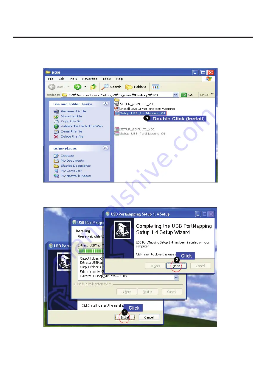
Page 110: ... Use Only Copyright 2011 LG Electronics Inc All right reserved Only for training and service purposes 5 DOWNLOAD 5 DOWNLOAD k G GaG㜼 Onzt s pG GZUWP XUj G G GGaG㜼 iyh psGO tnP YUGzV G 㾡 aG㜼 OGw 㾡 ㇵḴ㛺㢀UGP LG A230 LG A230 ...
Page 111: ...5 DOWNLOAD 111 LGE Internal Use Only Copyright 2011 LG Electronics Inc All right reserved Only for training and service purposes kss 㾡 a 㜼 On Y_W kssP kssG 㾡 aG㜼 On Y_W UkssP LG A230 LG A230 LG A230 ...
Page 112: ... 112 LGE Internal Use Only Copyright 2011 LG Electronics Inc All right reserved Only for training and service purposes 5 DOWNLOAD LG A230 LG A230 LG A230 ...
Page 113: ...5 DOWNLOAD 113 LGE Internal Use Only Copyright 2011 LG Electronics Inc All right reserved Only for training and service purposes z G zi w Gt G GGaGG㜼 OW P LG A230 ...
Page 114: ... 114 LGE Internal Use Only Copyright 2011 LG Electronics Inc All right reserved Only for training and service purposes 5 DOWNLOAD ziGk G 㾡 aG㜼 Osn zi t k G U U P ...
Page 115: ...5 DOWNLOAD 115 LGE Internal Use Only Copyright 2011 LG Electronics Inc All right reserved Only for training and service purposes ...
Page 116: ... 116 LGE Internal Use Only Copyright 2011 LG Electronics Inc All right reserved Only for training and service purposes 5 DOWNLOAD ziGt G 䈑 aG㜼OGpumpulvuGh Gz P O P LG A230 ...
Page 117: ...5 DOWNLOAD 117 LGE Internal Use Only Copyright 2011 LG Electronics Inc All right reserved Only for training and service purposes ...
Page 118: ... 118 LGE Internal Use Only Copyright 2011 LG Electronics Inc All right reserved Only for training and service purposes 5 DOWNLOAD 㐘䚽 䑀㢰 ⶸ㤸 aG㜼Ot nzt ZWP O P ...
Page 119: ...5 DOWNLOAD 119 LGE Internal Use Only Copyright 2011 LG Electronics Inc All right reserved Only for training and service purposes LG A230 LG A230 LG A230 LG A230 LG A230 LG A230 LG A230 LG A230 LG A230 ...
Page 120: ... 120 LGE Internal Use Only Copyright 2011 LG Electronics Inc All right reserved Only for training and service purposes 5 DOWNLOAD LG A230 LG A230 LG A230 LG A230 LG A230 LG A230 ...
Page 121: ...5 DOWNLOAD 121 LGE Internal Use Only Copyright 2011 LG Electronics Inc All right reserved Only for training and service purposes LG A230 LG A230 ...
Page 122: ... 122 LGE Internal Use Only Copyright 2011 LG Electronics Inc All right reserved Only for training and service purposes 5 DOWNLOAD LG A230 LG A230 ...
Page 123: ... 123 LGE Internal Use Only Copyright 2011 LG Electronics Inc All right reserved Only for training and service purposes 6 BLOCK DIAGRAM 6 BLOCK DIAGRAM ...
Page 124: ...IF2_RTS_N USIF2_CTS_N USIF1_TXD_MTSR USIF1_RXD_MRST USIF1_RTS_N USIF1_CTS_N DPLUS DMINUS XOX XO VSIM SIM_IO SIM_CLK SIM_RST MMCI_CMD MMCI_DAT_0 MMCI_CLK MMCI_DAT_1 MMCI_DAT_2 MMCI_DAT_3 SWIF_TXRX TDO TDI TMS TCK TRST_N TRIG_IN MON1 MON2 MON3 FSYS1 FSYS2 DIGUP_CLK DIGUP1 DIGUP2 LEDFBN LEDFBP LEDDRV A_D0 A_D1 A_D2 A_D3 A_D4 A_D5 A_D6 A_D7 A_D8 A_D9 A_D10 A_D11 A_D12 A_D13 A_D14 A_D15 A0 A1 A2 A3 A4 ...
Page 125: ...1 VA207 SEVY0005101 ICVL0518050FR C209 1u TP201 F p 9 3 2 5 2 C VA201 VA204 1u C203 C202 1u 1u C201 R217 0 C254 4 7p C200 1u F p 9 3 1 5 2 C SEVY0005101 ICVL0518050FR VA208 DNI R242 100 R230 R241 DNI 100n L202 5 0 2 A V 1 0 2 5 0 0 0 Y V E S 6 0 2 A V CN200 SUSY0028901 BRS 181213SL08 P 2 1 600 FB206 1 R245 R244 1 FB207 600 100 R231 0 033uF C243 K 2 2 2 3 2 R R229 2 2K VMAIN_MIC p 9 3 4 4 2 C R228 ...
Page 126: ... IO GND2 GND5 GND3 GND4 C304 0 1u VSIM_2V85 0 0 3 R K 7 4 0 5 1 9 2 3 R C301 22p VSIM_2V85 DNI C302 VSIM_2V85 C334 DNI DNI C335 VSIM_2V85 100K R318 DNI C314 KB319 VSIM_2V85 C313 22p 4 0 3 R K 7 4 VSIM_2V85 VA303 C329 1u 30 R330 VA301 VMMC_2V85 C316 0 1u 56K R323 R322 56K 56K R321 56K R320 56K R319 VDD_IO_1V8 R301 470 C328 2 2u C318 1u 8 V 1 _ G I D _ M A C V ENBY0034201 CN300 GB042 24S H10 E3000 1...
Page 127: ...01 2 3 1 FEED GND2 GND1 L404 1 8n C400 2 2u C421 100p TP400 ZD400 Q401 2 1 3 C412 1u 5 1ohms R402 R404 24K 22n L401 470n C415 C420 470n R412 4 7K 270ohms R408 270ohms R405 4 7K R411 C419 470n 5 1ohms R401 22n L402 24K R407 C413 1u 15p C418 L405 270n R400 15Kohms SFCY0000901 FL400 IN OUT GND1 GND2 DNI C409 C410 1n C405 10n VDD_IO_1V8 C403 10p 600 FB400 VAUX_2V85 C402 10p C401 10n VDD_IO_1V8 10n C40...
Page 128: ...ND13 PGND L504 2 7n L501 DNI 9 0 5 C p 8 1 L512 3 9n C511 0 5p L517 12n C518 6 8p 2 2n C522 C506 1n L514 15n 15n L515 C515 33p 1n C514 C507 39p 3 9n L513 L507 2 2nH 1K R501 ANT500 C516 1 2p L508 1 5n 2 2nH L505 L506 2 2nH VBAT L509 1 5n 1p C517 1n C508 C521 DNI 100p C523 L516 DNI 6 8n L511 C519 DNI C512 DNI L510 6 8n DNI L502 L503 DNI GND500 C513 1 2p C520 10u RF_TX_RAMP RF_HB_TX RF_LB_TX RF_HB_RX...
Page 129: ...A PIN MAP 129 LGE Internal Use Only Copyright 2011 LG Electronics Inc All right reserved Only for training and service purposes 8 BGA PIN MAP BGA IC pin check U101 ؼ Ball Diagram Top View PMB8815 not in use ...
Page 130: ... 130 LGE Internal Use Only Copyright 2011 LG Electronics Inc All right reserved Only for training and service purposes 8 BGA PIN MAP BGA IC pin check U301 ؼ Ball Diagram Top View H8BCS0QG0MMR ...
Page 131: ...KB318 KB306 KB311 KB316 2 0 3 N C K B 3 1 4 0 0 3 B K 0 1 3 B K 7 2 2 C 5 0 3 B K 1 0 3 D L 2 1 3 B K KB 1 3 7 3 1 3 B K LD303 R327 LD305 C326 R329 3 0 3 B K C327 LD302 R326 3 0 3 A V 2 0 3 A V LD304 R328 FB205 5 3 2 C 8 2 2 C 9 2 2 C VA202 1 3 2 C R216 C232 R214 R215 K B 3 1 5 K B 3 4 0 0 0 3 D L 4 2 3 R LG A230_MAIN_EAX64026401_1 1_TOP 9 PCB LAYOUT CON302 LCD PAD no Displaynd CON200 Speaker PAD ...
Page 132: ...100 C121 C122 6 4 1 C C106 L100 1 0 2 L 2 0 2 L 9 1 2 R 5 0 3 D Z 2 2 2 R 3 2 3 R R314 2 1 1 C C109 ZD306 R322 R223 R205 C337 3 0 3 L F R330 ZD304 VA301 5 0 3 L F R321 6 3 2 R R336 0 0 3 U 0 2 3 C 6 1 3 C C111 R309 C150 R310 3 1 1 C C110 R301 C140 8 2 1 C 1 3 2 R 3 0 1 C 0 3 2 R R229 C247 8 2 2 R C242 1 4 2 C 4 4 2 C 3 4 2 C 2 5 C 3 ANT500 4 6 2 C 9 0 5 L C208 4 0 2 C ZD200 L200 6 4 2 R FB200 2 4 ...
Page 133: ...ey Backlight 1 1 7 Speaker 1 1 8 Vibrator 1 1 8 Vibrator 1 1 9 Vibrator Duration Camera MicRcv Key Press Test SpeakerVibTest 2 Eng Mode 2 1 Call Timer 1 2 ELT Mode 1 2 1 Automatic 1 2 2 Manual 1 3 SW Sanity Test 1 3 1 FPRI Test 1 3 2 DB Check 1 3 3 E Serial NO 1 3 4 UA String 1 3 5 Unlock SIM 1 4 Factory Reset 1 5 Version 2 2 Eng Mode 2 2 1 Band Selection 2 2 1 1 Mattery Info 2 2 1 2 LCD Info 2 2 ...
Page 134: ...manual explains how to examine the status of RX and TX of the model A Tx Test TX test this is to see if the transmitter of the phones is activating normally B Rx Test RX test this is to see if the receiver of the phones is activating normally 11 2 Setting Method 1 Set COM Port 2 Check PC Baud Rate 3 Confirm EEPROM Delta file prefix name ྙ ԙ Ԛ 11 STAND ALONE TEST ...
Page 135: ...ONE TEST 135 LGE Internal Use Only Copyright 2011 LG Electronics Inc All right reserved Only for training and service purposes Not Connected ԛ Connected 4 Click Update Info for communicating Phone and Test Program ...
Page 136: ...eserved Only for training and service purposes 11 STAND ALONE TEST ԝ Ԝ Change ptest mood 5 For the purpose of the Standalone Test Change the Phone to ptest mode and then Click the Reset bar 6 Select Non signaling in the Quick Bar menu Then Standalone Test setup is finished ...
Page 137: ...LONE TEST 137 LGE Internal Use Only Copyright 2011 LG Electronics Inc All right reserved Only for training and service purposes 1 Non signaling mode bar and then confirm OK text in the command line 11 3 Tx Test Ԙ ...
Page 138: ...Inc All right reserved Only for training and service purposes 11 STAND ALONE TEST ྚ ྛ ྜ 2 Put the number of TX Channel in the ARFCN 3 Select Tx in the RF mode menu and PCL in the PA Level menu 4 Finally Click Write All bar and try the efficiency test of Phone ...
Page 139: ...yright 2011 LG Electronics Inc All right reserved Only for training and service purposes 11 4 Rx Test 1 Put the number of RX Channel in the ARFCN 2 Select Rx in the RF mode menu 3 Finally Click Write All bar and try the efficiency test of Phone ԙ Ԙ Ԛ ...
Page 140: ...LG Electronics Inc All right reserved Only for training and service purposes 11 STAND ALONE TEST ԛ Ԝ Change normal mode 4 The Phone must be changed normal mode after finishing Test 5 Change the Phone to normal mode and then Click the Reset bar ...
Page 141: ...d Battery Calibration with Agilent 8960 GSM call setting instrument and Tektronix PS2521G Programmable Power supply Auto cal generates calibration data by communicating with phone and measuring equipment then write it into calibration data block of flash memory in GSM phone 12 2 Directory structure of Tachyon C LGE Tachyon 12 AUTO CALIBRATION 12 AUTO CALIBRATION 12 1 Overview 12 2 Directory struct...
Page 142: ...for communication with system Config ini configuration files for port setting and cable loss Model configuration files for each model OCX component files for Tachyon PhoneCmd files for communication with phone Report test result files Temp store calibration value 12 3 2 File Explain Model_Calibration xml stored data for calibration Model_CallSetuo xml stored equipment setting data for auto test Mo...
Page 143: ...e Only Copyright 2011 LG Electronics Inc All right reserved Only for training and service purposes 12 AUTO CALIBRATION 12 4 Procedure 1 Execute LGE Tachyon Tachyon Exe and Click Login button 2 Tachyon execute ready display ...
Page 144: ... 12 AUTO CALIBRATION 12 5 Tachyon Main UI 1 Model Selection 2 Calibration Test 3 Not Support 4 Stop 5 Test Only 6 Calibration Only 7 Phone Control 8 Loss Adjustment 9 System Option 10 Run Option 11 Voltage Current Setting 12 Show Result 12 5 1 Tool bar 12 5 2 Command button Only support Calibration Test and Stop button ...
Page 145: ...can get proper scale factor value and measured power level 11 8 ADC This procedure is for battery calibration You can get main Battery Config Table and temperature Config Table will be reset 11 9 Target Power 29 5 dBm 29 5 dBm 29 5 dBm Max power 1909 8 MHz 1880 MHz 1850 2 MHz Frequency 810 661 512 Channel PCS 1900 29 5 dBm 29 5 dBm 29 5 dBm Max power 1784 8 MHz 1747 6 MHz 1710 2 MHz Frequency 885 ...
Page 146: ... SUMY00 ABM00 SJMY00 ABA00 EBP00 EAB00 Location Description GGZZ00 Screw Tapping ACQ00 Cover Assembly Front MJN00 Tape Window MKC00 Window LCD ACQ01 Cover Assembly Rear EAA00 PIFA Antenna Multiple EBR00 PCB Assembly Main ABA00 Bracket Assembly ABM00 Can Assembly Shield SUMY00 Microphone Condenser SJMY00 Motor DC ADB00 Dome Assembly Metal EAB00 Speaker Dual Mode EAJ00 LCD Module TFT EBP00 Camera Mo...
Page 147: ...32701 Cover Front MCK66669201 MOLD PC LEXAN141R LGA230 AINDZY BK Black 4 MCQ043301 Damper LCD MCQ66589201 COMPLEX LGA230 AINDZY ZZ Without Color 4 MDJ000001 Filter MDJ63105801 COMPLEX LGA230 AINDZY ZZ Without Color 4 MDJ000002 Filter MDJ63105901 COMPLEX LGA230 AINDZY ZZ Without Color 4 MJN00 Tape Window MJN67751601 COMPLEX LGA230 AINDZY ZZ Without Color 4 MKC00 Window LCD MKC63980201 CUTTING PMMA ...
Page 148: ...N 4 EBR071500 PCB Assembly Main Insert EBR73886701 LGA230 AINDKG 1 0 Main 5 ABA00 Bracket Assembly ABA73929201 LGA230 AINDZY ZZ Without Color 6 MAZ000000 Bracket MAZ63106501 MOLD PC LEXAN141R LGA230 AINDZY ZZ Without Color SPK BRACKET 6 MCQ074200 Damper Speaker MCQ66589501 COMPLEX LGA230 AINDZY ZZ Without Color pad speaker 6 MJN009400 Tape Camera MJN67751501 COMPLEX LGA230 AINDZY ZZ Without Color ...
Page 149: ... AINDZY 1 0 MAIN 5 EBR071600 PCB Assembly Main SMT Bottom EBR72889801 LGA230 AINDZY 1 1 MAIN 5 MEZ000000 Label MLAZ0038301 COMPLEX LG VX6000 ZZ Without Color PID Label 4 Array PRINTING 5 EBR071700 PCB Assembly Main SMT Top EBR72889901 LGA230 AINDZY 1 0 MAIN 6 EAX010000 PCB Main EAX64026401 EAX64026401 LGA230 AINDZY 1 0 FR 4 SBL 6 10 Main LG Innotek com 3 AEX00 Keypad Assembly Main AEX73698101 LGA2...
Page 150: ...STER BOX for CGR TDR 2VER mbox_label GSM standard_master box label 2 MLAP Label Unit MLAP0001138 PRINTING LG RD6100 RLC ZZ Without Color GSM standard_Seal label 2 MLAQ Label Unit Box MLAQ0015213 PRINTING KG270 INDBK ZZ Without Color GSM MRP LABEL Made by LGE 100 48 IND MRP_unit box label 2 MLAZ00 Label MLAZ0050901 COMPLEX KU990 GBRBK ZZ Without Color 1 AAD000000 Addition Assembly AAD85818901 LGA23...
Page 151: ...URATA MANUFACTURING CO LTD 6 L510 L511 Inductor Multilayer Chip ELCH0001408 LL1005 FHL6N8J 6 8NH 5 300mA 0 23OHM 5 6GHZ 9 SHIELD NONE 1 0X0 5X0 5MM R TP TOKO INC 6 R201 R219 Resistor Chip ERHZ0000407 MCR01MZP5J105 1MOHM 5 1 16W 1005 R TP ROHM 6 C109 C115 C116 C126 C132 C200 C201 C202 C203 C240 C317 C318 C319 C320 C322 C323 C331 C412 C413 Capacitor Ceramic Chip ECCH0004904 GRM155R60J105K 1uF 10 6 3...
Page 152: ...ANUFACTURING CO LTD 6 C259 C418 Capacitor Ceramic Chip ECCH0000112 MCH155C150J 15pF 5 50V NP0 55TO 125C 1005 R TP ROHM Semiconductor KOREA CORPORATION 6 R111 R112 R113 R118 R237 R239 R314 R315 R318 R332 R334 R406 R417 Resistor Chip ERHZ0000406 MCR01MZP5J104 100KOHM 5 1 16W 1005 R TP ROHM 6 C407 Capacitor Ceramic Chip ECZH0000803 C1005C0G1H020CT000F 2pF 0 25PF 50V NP0 55TO 125C 1005 R TP TDK KOREA ...
Page 153: ...C 1005 R TP ROHM Semiconductor KOREA CORPORATION 6 C242 C244 C245 C247 C251 C252 C507 Capacitor Ceramic Chip ECCH0000120 MCH155A390J 39pF 5 50V NP0 55TO 125C 1005 R TP ROHM Semiconductor KOREA CORPORATION 6 C209 C249 Capacitor Ceramic Chip ECZH0003503 GRM188R61E105K 1uF 10 25V X5R 55TO 85C 1608 R TP MURATA MANUFACTURING CO LTD 6 R117 R333 R414 Resistor Chip ERHY0000241 MCR01MZP5J102 1KOHM 5 1 16W ...
Page 154: ... MCH155A470JK 47pF 5 50V NP0 55TO 125C 1005 R TP ROHM Semiconductor KOREA CORPORATION 6 R244 R245 Resistor Chip ERHZ0000434 MCR01MZP5J1R0 1OHM 5 1 16W 1005 R TP ROHM 6 FL303 FL304 FL305 Filter EMI Power SFEY0013201 EVRC14S03Q030100R ESD EMI 0HZ 15pF 0H SMD R TP AMOTECH CO LTD 6 C119 C205 C210 C211 C212 C213 C215 C219 C220 C223 C321 C329 C332 Capacitor Ceramic Chip ECZH0001215 C1005X5R1A105KT000F 1...
Page 155: ...008105 BLM15BD182SN1D 1800 ohm 1 0X0 5X0 5 25 1 4 ohm 0 1A SMD R TP 2P 0 MURATA MANUFACTURING CO LTD 6 C107 C111 C146 Capacitor Ceramic Chip ECZH0001216 C1005X5R1A224KT000E 220nF 10 10V X5R 55TO 85C 1005 R TP TDK KOREA COOPERATION 6 R233 Resistor Chip ERHZ0000295 MCR01MZP5F5102 51KOHM 1 1 16W 1005 R TP ROHM 6 U200 IC Mini ABB EAN62112401 RT8966AGQW RT8966A 1 65 5 5V 60uA SWITCH MULTIPLEXER QFN R T...
Page 156: ...DB 28DB 39 39 37 37 50UA 1 46A 970mA 33DB 33DB 45DBM 1 3DBM 28P 6 0x6 0x1 0MM SKYWORKS SOLUTIONS INC 6 L505 L506 L507 Inductor Multilayer Chip ELCH0004721 1005GC2T2N2SLF 2 2NH 0 3NH 300mA 0 16OHM 6GHZ 8 SHIELD NONE 1 0X0 5X0 5MM R TP PILKOR ELECTRONICS LTD 6 R101 R301 R302 R303 R305 R306 R307 R308 R309 R310 Resistor Chip ERHZ0000484 MCR01MZP5J471 470OHM 5 1 16W 1005 R TP ROHM 6 R235 R238 R248 Resi...
Page 157: ...1 LSCR523EBFS8 NPN 5V 50V 50V 100mA 100NA 120 560 150mW EMT3 R TP 3P ROHM Semiconductor KOREA CORPORATION 6 L504 Inductor Multilayer Chip ELCH0001039 HK1005 2N7S T 2 7NH 0 3NH 300mA 0 13OHM 6GHZ 8 SHIELD NONE 1 0X0 5X0 5MM R TP TAIYO YUDEN CO LTD 6 R228 R501 Resistor Chip ERHZ0000404 MCR01MZP5J102 1KOHM 5 1 16W 1005 R TP ROHM 6 C234 Capacitor Ceramic Chip ECCH0000182 GRM155R61A104K 0 1uF 10 10V X5...
Page 158: ...CS R 1 71 5 5V 0W WLCSP R TP 20P WOLFSON MICROELECTRONICS PLC 6 L509 Inductor Multilayer Chip ELCH0001033 HK1005 1N5S T 1 5NH 0 3NH 300mA 0 1OHM 6GHZ 8 SHIELD NONE 1 0X0 5X0 5MM R TP TAIYO YUDEN CO LTD 6 C511 Capacitor Ceramic Chip ECZH0001002 C1005CH1H0R5BT000F 0 5pF 0 1PF 50V NP0 55TO 125C 1005 R TP TDK KOREA COOPERATION 6 C253 Capacitor Ceramic Chip ECCH0007802 CL10A475KP8NNNC 4 7uF 10 10V X5R ...
Page 159: ...ATA MANUFACTURING CO LTD 6 R405 R408 Resistor Chip ERHZ0000531 MCR01MZP5J271 270OHM 5 1 16W 1005 R TP ROHM 6 R104 Resistor Chip ERHZ0000499 MCR01MZP5J562 5 6KOHM 5 1 16W 1005 R TP ROHM 6 Q400 Q401 TR Bipolar EBK61573301 2SC5086 NPN 3V 20V 12V 80mA 1UA 80 160 100mW 2 2H1B R TP 3P TOSHIBA ELECTRONICS KOREA CORPORATION 6 R404 R407 Resistor Chip ERHZ0000449 MCR01MZP5J243 24KOHM 5 1 16W 1005 R TP ROHM ...
Page 160: ...3MG0 3 3 uH N 2x2 5x1 0 R TP chip power MURATA MANUFACTURING CO LTD 6 SC200 Can Shield MCBA0059201 COMPLEX GD350 CLP ZZ Without Color 6 J200 Jack Phone ENJE0008001 JAM3333 F32 7F 1P 4P ANGLE R TP 4mM BLACK 6P HON HAI PRECISION INDUSTRY CO LTD 6 VA207 VA208 Varistor SEVY0005101 ICVL0518050FR 18V 0 5F 1 0 0 5 0 55 NONE SMD R TP INNOCHIPS TECHNOLOGY 6 CN202 Connector Terminal Block EAG62832501 KQ03LV...
Page 161: ...C213 C215 C219 C220 C223 C321 C329 C332 Capacitor Ceramic Chip ECZH0001215 C1005X5R1A105KT000F 1uF 10 10V X5R 55TO 85C 1005 R TP TDK KOREA COOPERATION 6 C328 C400 C404 Capacitor Ceramic Chip ECCH0000198 CL05A225MQ5NSNC 2 2uF 20 6 3V X5R 55TO 85C 1005 R TP SAMSUNG ELECTRO MECHANICS CO LTD 6 R117 R333 R414 Resistor Chip ERHY0000241 MCR01MZP5J102 1KOHM 5 1 16W 1005 R TP ROHM 6 R324 R325 R326 R327 R32...
Page 162: ...ation No Description PartNumber Spec Remark 6 FB200 FB201 FB202 FB203 FB204 Filter Bead SFBH0008105 BLM15BD182SN1D 1800 ohm 1 0X0 5X0 5 25 1 4 ohm 0 1A SMD R TP 2P 0 MURATA MANUFACTURING CO LTD 6 R214 Resistor Chip ERHZ0000529 MCR01MZP5J152 1 5KOHM 5 1 16W 1005 R TP ROHM 6 R114 R115 R208 R229 R232 Resistor Chip ERHZ0000443 MCR01MZP5J222 2 2KOHM 5 1 16W 1005 R TP ROHM ...
Page 163: ...t Color 3 MFL053800 Manual Operation MFL67213401 COMPLEX LGA230 AINDKG ZZ Without Color LGA230 manual for IND 2 EAB010200 Earphone Stereo SGEY0003744 EMB LGE004MSKB 3mW 16OHM 115DB 85HZTO126HZ 1M BLACK 3 5 L TYPE STEREO 4POLE PLUG CRESYN CO LTD 2 EAY060000 Adapters SSAD0032601 STA U34ID STA U34ID 100 240V 5060 Hz 5 1 V 0 7 A CE AC DC ADAPTOR DONG DO ELECTRONICS CO LTD 2 EAC00 Rechargeable Battery ...