3. TECHNICAL BRIEF
- 18 -
(3) Digitally-controlled crystal oscillator
The Aero II transceiver integrates the DCXO circuitry required to generate a precise system reference clock
using only an external crystal resonator. The DCXO replaces a discrete VC-TCXO module. The DCXO
allows for the use of a standard 26 MHz crystal, which reduces both cost and area compared to using a
VCTCXO module. There are no external varactors or trim capacitors required. This simplifies the design,
programming, and manufacturing compared to less integrated solutions.
The DCXO uses the CDAC and CAFC arrays to correct for both static and dynamic frequency errors,
respectively. An internally digitally programmable capacitor array (CDAC) provides a coarse method of
adjusting the reference frequency in discrete steps. The CDAC[6:0] bits in Register 03h are programmed to
compensate for static variations in PCB design, manufacturing, and crystal tolerance, and are typically set
to center the oscillator frequency during production. A second capacitor array (CAFC) allows for fine and
continuous dynamic adjustment of the reference frequency by an external control voltage (AFC). This
control voltage is supplied by the AFC DAC of the baseband and should be connected to the transceiver
AFC pin (pin 27). The baseband determines the appropriate frequency adjustment based on the receipt of
the FCCH burst. The baseband then adjusts the AFC voltage to correct for frequency variations caused by
temperature drift.
The transceiver can be adjusted for the corresponding baseband AFC input full-scale voltage by setting the
AFCREF bit in Register 04h. Additionally, the Aero II transceiver supports an optional Digital AFC mode for
DCXO operation that is selected by the AFCC bit in Register 04h. In digital mode, the connection between
the baseband and transceiver is eliminated. AFC control is performed directly by a register write operation.
This has the benefit of further easing PCB design and enabling a DAC in the baseband to be allocated to
another function.
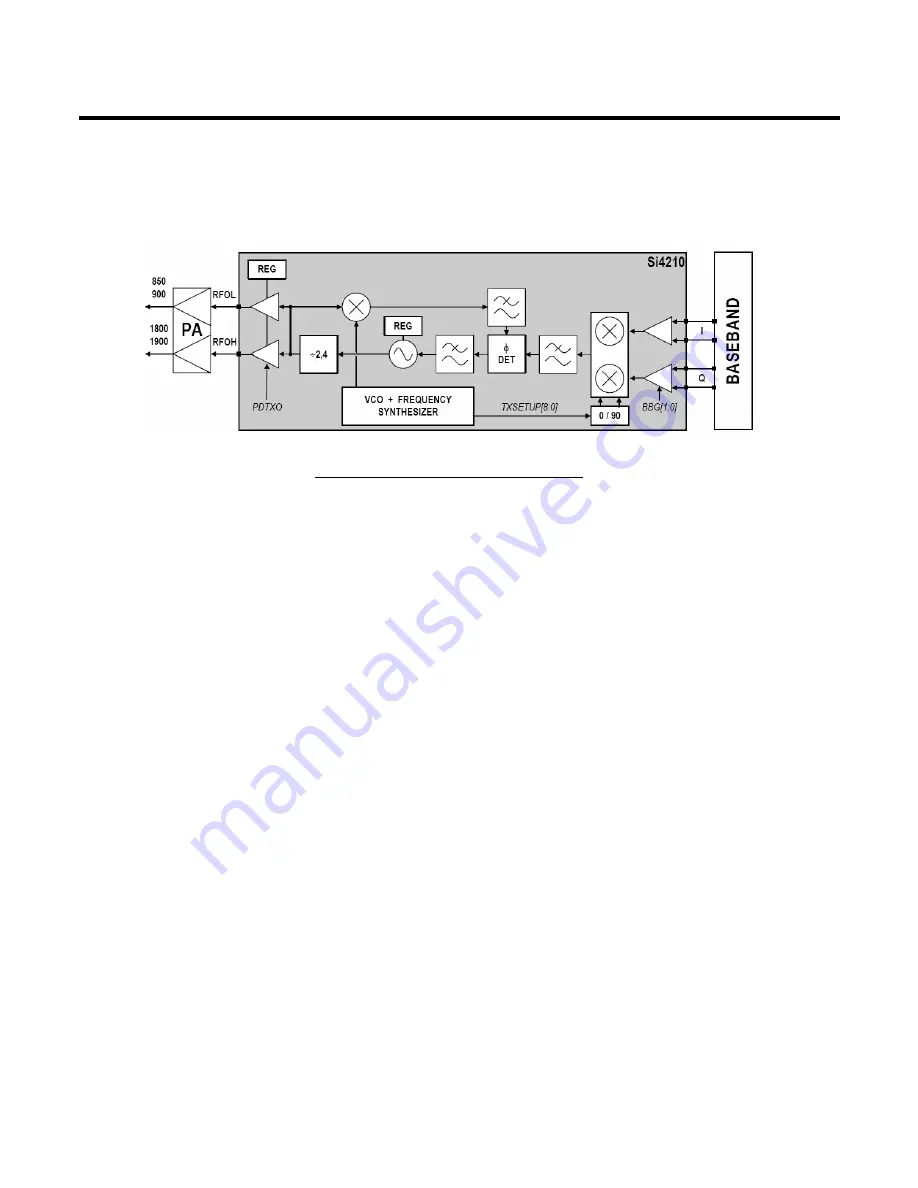
Figure. 3-3 SI4210 TRANSMITTER PART
Summary of Contents for KG320
Page 1: ...Date May 2006 Issue 1 0 Service Manual Model KG320 Service Manual KG320 ...
Page 3: ... 4 ...
Page 20: ...3 TECHNICAL BRIEF 21 Figure 3 5 SKY77328 FUNCTIONAL BLOCK DIAGRAM ...
Page 39: ...3 TECHNICAL BRIEF 40 3 7 CAMERA IC AIT811T U103 Figure 3 18 AIT811T APPLICATION BLOCKDIAGRAM ...
Page 41: ...3 TECHNICAL BRIEF 42 3 8 MIDI IC YMU787 U202 Figure 3 20 YMU787 BLOCKDIAGRAM ...
Page 72: ...4 TROUBLE SHOOTING 73 4 6 LCD Trouble AIT811T EMI FILTER CN102 TEST POINT Figure 4 6 ...
Page 90: ...4 TROUBLE SHOOTING 91 4 14 Camera and Flash Trouble Camera Module U201 CN202 Figure 4 17 ...
Page 99: ... 100 ...
Page 107: ... 108 8 PCB LAYOUT ...
Page 108: ... 109 8 PCB LAYOUT ...
Page 109: ... 110 8 PCB LAYOUT ...
Page 110: ... 111 8 PCB LAYOUT ...
Page 111: ... 112 8 PCB LAYOUT ...
Page 112: ... 113 8 PCB LAYOUT ...
Page 113: ... 114 ...
Page 121: ...10 STAND ALONE TEST 122 Figure 10 2 HW test setting Figure 10 3 Ramping profile ...
Page 127: ... 128 ...
Page 129: ... 130 ...
Page 147: ...Note ...
Page 148: ...Note ...


