


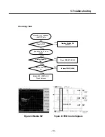


5. Trouble shooting
- 112 -
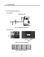
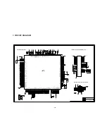
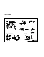
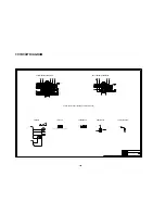
5.12.13 Checking FEM & Mobile SW
Circuit Diagram
Checking Points
Mobile SW & FEM
Figure 30. Mobile SW & FEM Circuit
Figure 31 Mobile SW & FEM Input
L408
2.7nH
0.1u
C437
R406
0
ANT
G1
G2
RF
SW401
KMS-506
C404
100p
2V85_RF
10p
C462
6
TX2G
8
VCTRL1
22
21
VCTRL2
20
VCTRL3
3
VDD
EGSM_RX-
18
GMS_RX-
2
GND1
25
GND10
GND11
26
4
GND2
GND3
5
7
GND4
GND5
9
10
GND6
11
GND7
GND8
23
GND9
24
19
13
12
PCS_RX-
TX1G
FL308
YGHF-S006A
ANT
1
15
14
DCS_RX-
17
16
FL30
SW40
R403
R405
R441
R40
Table 5. FEM TX Control Logic
RX Mode
EGSM
DCS
PCS
ANT_SW1
On
On
On
ANT_SW2
Off
On
On
ANT_SW3
Off
Off
Off
Summary of Contents for KE820
Page 1: ...Service Manual Model KE820 Service Manual KE820 Date August 2006 Issue 1 0 ...
Page 3: ... 4 ...
Page 5: ... 6 ...
Page 46: ...3 TECHNICAL BRIEF 47 Figure 18 EN SET port control method ...
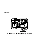
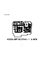
Page 69: ...4 PCB layout 70 Figure 45 Main PCB bottom Figure 46 Main PCB bottom placement ...
Page 70: ...4 PCB layout 71 Figure 47 Sub PCB top Figure 48 Sub PCB top placement ...
Page 71: ...4 PCB layout 72 Figure 49 Sub PCB bottom Figure 50 Sub PCB bottom placement ...
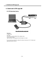
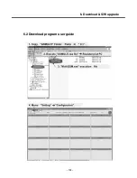
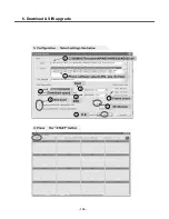
Page 114: ...6 Download S W upgrade 115 6 2 Download program user guide ...
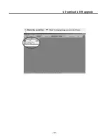
Page 115: ... 116 6 Download S W upgrade ...
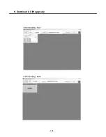
Page 116: ... 117 6 Download S W upgrade ...
Page 117: ... 118 6 Download S W upgrade ...
Page 124: ... 125 8 PCB LAYOUT ...
Page 125: ... 126 8 PCB LAYOUT ...
Page 126: ... 127 8 PCB LAYOUT ...
Page 127: ... 128 8 PCB LAYOUT ...
Page 141: ... 142 ...
Page 161: ...Note ...
Page 162: ...Note ...


