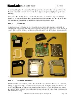
4-19
PIN NO
PIN NAME
TYPE
DESCRIPTION
LDD serial interface (3)
44
LDD_SDIO
LDD serial interface data. The pin is spike-free at power-on stage.
45
LDD_CLK
LDD serial interface CLK. The pin is spike-free at power-on stage.
46 LDD_SEN
LDD serial interface command enable.
The pin is spike-free at power-on stage.
Panel & sense key (5)
Tray_is_in Input, A Logical Low Indicates the Tray is IN.
67
TRAYIN
Feedback Flag is from Tray Connector.
The pin is spike-free at power-on stage.
Tray_is_out Input. A Logical Low Indicates the Tray is OUT.
68
TRAYOUT
Feedback Flag is from Tray Connector.
The pin is spike-free at power-on stage.
69 EJECT
Eject/stop key input, active low.
The pin is spike-free at power-on stage.
Sledge Inner Limit Input, Active Low.
72
LIMIT
The pin is spike-free at power-on stage.
Alternate function : 1. Internal monitored signal output
73 PLAY
Play/pause key input, active low.
The pin is spike-free at power-on stage.
MISC & GIO function (21)
120
RSTI
Analog Input
Internal power on reset detection input.
3.3V LVTTL I/O,
62 GIO12
5V-tolerance,
General IO
4,8,12,16mA
PDR,
75K
pull-up
63
GIO13
General
IO.
65 GIO0/MUTE1
General
IO
66 GIO1/MUTE2
General
IO
LED Control Output. Initial 0 Output.
70
LED1/GIO3
The pin is spike-free at power-on stage.
Alternate function : General I/O
87
GIO4
3.3V LVTTL I/O
General IO.
88
GIO5
3.3V LVTTL I/O
General IO.
89
GIO6
3.3V LVTTL I/O
General IO.
90
GIO7/MUTE3
General IO. The pin is spike-free at power-on stage.
91
GIO8
General
IO.
General IO.The pin is spike-free at power-on stage.
92
GIO9/SPOKE
The pin is not allowed to pull-up in circuit layout.
Alternate function : Spoke input.
PC RS232 serial receive data.
93
RXD_A/
The pin is spike-free at power-on stage.
LED2/GIO10
Alternate function : 1. LED Control Output. Initial “0” Output
2. General IO.
PC RS232 serial transmit data.
94 TXD_A/GIO11
The pin is spike-free at power-on stage.
Alternate function : 1. LED Control Output. Initial “0” Output
2. General IO.
95
GIO2
General
IO
103
GIO14
General
IO
104
GIO19
General
IO
105
GIO16
General
IO
106
GIO17
General
IO
107
GIO18
General
IO
108
GIO15
General IO The pin is not allowed to pull-up in circuit layout.
Digital Power Pins (11)
60,61,112
DVDD33O
Digital Power (3.3V) VDD for digital pad.
109,114
MVDDQ
DRAM Power (3.3V) VDD for pad output buffer of DRAM die.
111,113
MVSSQ
DRAM Ground
VSS for pad output buffer of DRAM die.
59,71,
110,115
DVDD12I
Digital Power (1.2V) VDD for internal circuit.
64
VSS
Digital Ground
VSS for digital pad
3.3V LVTTL I/O,
5V-tolerance,
2,4,6,8mA PDR,
75K pull-up
3.3V LVTTL I/O,
5V-tolerance,
12mA,75K pull-up
3.3V LVTTL I/O,
5V-tolerance,
4,8,12,16mA PDR,
75K pull-down
3.3V LVTTL I/O,
5V-tolerance,
4,8,12,16mA PDR,
75K pull-down
Summary of Contents for HB954TB
Page 51: ...2 42 WAVEFORMS 1 SYSTEM PART 1 X500 27MHz 1 X501 25MHz 2 1 IC500 BCM7440P 2 ...
Page 53: ...2 44 3 VIDEO PART 1 100 FULL COLOR BAR CVBS_I 7 Y 8 Pb 9 Pr 10 7 9 10 8 ...
Page 54: ...2 45 4 VIDEO PART 2 100 FULL COLOR BAR CVBS 11 COMP_Y 12 COMP_Pb 13 COMP_Pr 14 11 14 12 13 ...
Page 55: ...2 46 5 HDMI PART HDMI_SDA 15 HDMI_SCL 16 HDMI_CLK 17 HDMI_DATA 18 18 17 15 16 ...
Page 56: ...2 47 6 MICOM AND MPEG I F PART T_TX 19 R_RX 20 20 19 ...
Page 57: ...2 48 MEMO ...
Page 80: ...2 93 2 94 PRINTED CIRCUIT BOARD DIAGRAMS 1 MAIN P C BOARD TOP VIEW ...
Page 81: ...2 95 2 96 MAIN P C BOARD BOTTOM VIEW ...
Page 82: ...2 97 2 98 2 SMPS P C BOARD TOP VIEW ...
Page 83: ...2 99 2 100 SMPS P C BOARD BOTTOM VIEW ...
Page 84: ...2 101 2 102 3 AMP P C BOARD TOP VIEW BOTTOM VIEW ...
Page 87: ...3 2 MEMO ...
Page 93: ...3 10 ...
Page 94: ...954B 954A 950 955 956 957 951 958 953 952 A900 4 3 PASSIVE SUBWOOFER SB94TB W 3 11 ...
Page 95: ...MEMO 3 12 ...
Page 117: ...4 22 MEMO ...
Page 118: ...4 24 4 23 CIRCUIT DIAGRAM LOADER HL 04P EBY51750301 REV 6 1 2009 01 20 ...
Page 120: ...4 27 4 28 PRINTED CIRCUIT BOARD DIAGRAMS TOP VIEW ...
Page 121: ...4 29 4 30 BOTTOM VIEW ...