13
3.1.1 Overview of X-GOLDTM102
The X-GOLDTM102 is a GSM baseband modem including RF transceiver covering the low
bands GSM850 / GSM900 and high bands GSM1800 / GSM1900 bands. X-GOLDTM102 is Dual
Band, therefore, it supports by default a low / high pair of bands at the same time:
1. GSM850 / GSM1800
2. GSM850 / GSM1900
3. GSM900 / GSM1800
4. GSM900 / GSM1900.
The X-GOLDTM102 is optimized for voice-centric Mobile Phone applications.
The X-GOLDTM102 is designed as a single chip solution that integrates the digital, mixed-signal,
RF functionality and a direct-to-battery Power Management Unit.
The transceiver consists of:
• Constant gain direct conversion receiver with an analog I/Q baseband interface
• Fully integrated Sigma/Delta-synthesizer capability
• Fully integrated two-band RF oscillator
• Two-band digital GMSK modulator with digital TX interface
• Digitally controlled crystal oscillator generating system clocks.
The X-GOLDTM102 supports a direct to battery connection, hence eliminating the need for an
external Power Management Unit. The X-GOLDTM102 has different power down modes and an
integrated power up sequencer.
The X-GOLDTM102 is powered by the C166®S-V2 MCU and TEAKLite® DSP cores. The
operating temperature range from -30°C to 85°C. It is manufactured using the 0.13
μ
m CMOS
process.
3.1.2 Features
Baseband
• High performance fixed-point TEAKlite DSP
• C166S-V2 high performance microcontroller with a 16KB Instruction Cache and a Data cache
Buffer.
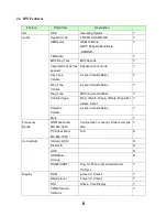
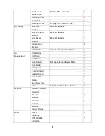
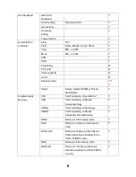
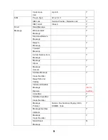
• There are several Interfaces:
– I2S interface for DAI connections (for Tape Approval) and external Audio component connection.
– High Speed SSC Interface for connection of companion chips (like Serial SD Cards)
– High Speed SSC Interface dedicated to Display control
– USIM Interface with support of Protocol T=1
– Keypad Interface (6x4 or 5x5 keys)
– EBU for external RAM/NOR FLASH/Busrt Flash/NAND Flash/Parallel Display connection
– Asynchronous serial interface.
– Asynchronous serial interface for WLAN/BT/GPS control (incl. IrDA support capability) .
– JTAG Interface, OCDS, Multi-Core Debug and Real Time Trace facilities.
– Black & white and color displays are supported
Summary of Contents for GB130kf750
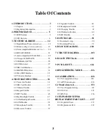
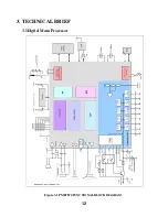
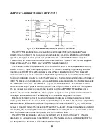
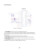
Page 12: ...12 3 TECHNICAL BRIEF 3 1Digital Main Processor Figure 3 1 PMB7890 FUNCTIONAL BLOCK DIAGRAM ...
Page 28: ...28 ...
Page 29: ...29 Pin Description ...
Page 35: ...35 Circuit Diagram TP1 TP6 TP2 TP4 TP 3 TP5 ...
Page 36: ...36 Checking Flow ...
Page 37: ...37 4 2 SIM Card Trouble Test Point Circuit Diagram ...
Page 38: ...38 Checking Flow ...
Page 39: ...39 4 3 Vibrator Trouble Test Point Circuit Diagram ...
Page 40: ...40 Checking Flow NG ...
Page 41: ...41 4 4 Keypad Trouble Test Point ...
Page 42: ...42 Circuit Diagram ...
Page 43: ...43 ...
Page 44: ...44 Checking Flow ...
Page 45: ...45 4 5 RTC Trouble Test Point Circuit Diagram ...
Page 46: ...46 Checking Flow ...
Page 47: ...47 4 6 Key Backlight Trouble 4 6 1 Main Key Board LED ...
Page 48: ...48 Circuit Diagram Checking Flow ...
Page 49: ...49 4 6 2 Upper Key Board LED Circuit Diagram TP1 ...
Page 50: ...50 Checking Flow ...
Page 51: ...51 4 7 LCM Backlight Trouble Test Point Circuit Diagram ...
Page 52: ...52 Checking Flow ...
Page 53: ...53 4 8 LCM Trouble Test Point Circuit Diagram ...
Page 54: ...54 Checking Flow ...
Page 55: ...55 4 9 Microphone Trouble Test Point Circuit Diagram TP1 ...
Page 56: ...56 Checking Flow ...
Page 57: ...57 4 10 Receiver Trouble Test Point ...
Page 58: ...58 Circuit Diagram ...
Page 59: ...59 Checking Flow ...
Page 60: ...60 4 11Speaker Trouble Test Point ...
Page 61: ...61 Circuit Diagram ...
Page 62: ...62 Checking Flow ...
Page 63: ...63 4 12 Headphone Trouble Test Point Circuit Diagram ...
Page 64: ...64 ...
Page 65: ...65 Checking Flow ...
Page 66: ...66 ...
Page 67: ...67 4 13 Charging Trouble Test Point Circuit Diagram TP1 TP4 TP3 TP5 TP2 ...
Page 68: ...68 Checking Flow ...
Page 69: ...69 4 14 FM Radio Trouble Test Point ...
Page 70: ...70 Circuit Diagram ...
Page 71: ...71 Checking Flow ...
Page 72: ...72 ...
Page 74: ...74 RF Trouble TEST POINT ...
Page 76: ...76 ...
Page 77: ...77 RX Trouble TEST POINT ...
Page 78: ...78 CIRCUIT TP5 TP6 TP3 TP4 TP1 TP2 ...
Page 79: ...79 CHECKING FLOW ...
Page 80: ...80 TEST POINT CIRCUIT TP1 TP2 TP5 TP6 TP3 TP4 TP2 TP1 ...
Page 81: ...81 WAVE FORM CHECKING FLOW Replace X301 ...
Page 82: ...82 TX Trouble TEST POINT ...
Page 83: ...83 CIRCUIT WAVE FORM TP5 TP6 TP3 TP4 TP2 TP1 ...
Page 84: ...84 TEST POINT ...
Page 85: ...85 CHECKING FLOW ...
Page 86: ...86 Signal configuration CHECKING FLOW ...
Page 87: ...87 TROUBLE SHOOTING TEST POINT CIRCUIT TP5 TP6 TP3 TP4 TP1 TP2 ...
Page 88: ...88 WAVE FORM ...
Page 89: ...89 CHECKING FLOW ...
Page 90: ...90 5 DOWNLOAD 5 1 Download Setup ...
Page 100: ...100 3 DownLoad Fail If download fail that it will show red and display progress in log window ...
Page 101: ...101 Fig 2 DownLoad success DownLoad Pass will display green color ...
Page 102: ...102 6 BLOCK DIAGRAM ...
Page 103: ...103 7 CIRCUIT DIAGRMA ...
Page 104: ...104 ...
Page 105: ...105 ...
Page 106: ...106 ...
Page 107: ...107 ...
Page 108: ...108 ...
Page 109: ...109 ...
Page 110: ...110 ...
Page 111: ...111 ...
Page 112: ...112 8 BGA IC PIN Check 8 1 BGA PIN Check of MCU PMB7890 BGA use BGA non use ...
Page 113: ...113 8 2 BGA PIN Check of Memory S71GL064NA0BFW0Z0 BGA use BGA non use ...
Page 137: ...137 13 EXPLODED VIEW REPLACEMENT PART LIST 13 1 EXPLODED VIEW ...
Page 138: ...138 Ass y exploded view ...


