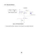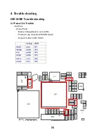
22
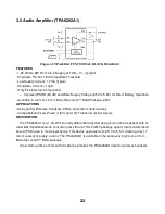
3.5 Audio Amplifier (TPA6202A1)
Figure.3-5 TPA6202A1 FUNCTIONAL BLOCK DIAGRAM
FEATURES
·
1.25 W Into 8W From a 5-V Supply at THD = 1% (Typical)
·
Shutdown Pin has 1.8V Compatible Threshold
·
Low Supply Current: 1.7mA Typical
·
Shutdown Current < 10
µ
A
·
Only Five External Components
–
Improved PSRR (90 dB) and Wide Supply Voltage (2.5V to 5.5V) for Direct Battery Operation
·
Avaliable in a 2 mm x 2 mm MicroStar Junior™ BGA Package (ZQV
)
APPLICATIONS
·
Designed for Wireless Handsets, PDAs, and other mobile devices
·
Compatible with Low Power (1.8V Logic) I/O Threshold control signals
DESCRIPTION
The TPA6202A1 is a 1.25-W mono fully differential amplifier designed to drive a speaker with at
least 8-
Ώ
impedance while consuming less than 37 mm2 (ZQV package option) total printed-circuit
board (PCB) area in most applications. This device operates from 2.5 V to 5.5 V, drawing only 1.7
mA of quiescent supply current. The TPA6202A1 is available in the space-saving 2 mm x 2 mm
MicroStar Junior™ BGA package.
A fast start-up time of 4ms with minimal pop makes the TPA6202A1 ideal for wireless handsets.
Summary of Contents for GB130kf750
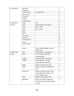
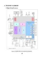
Page 12: ...12 3 TECHNICAL BRIEF 3 1Digital Main Processor Figure 3 1 PMB7890 FUNCTIONAL BLOCK DIAGRAM ...
Page 28: ...28 ...
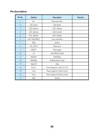
Page 29: ...29 Pin Description ...
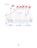
Page 35: ...35 Circuit Diagram TP1 TP6 TP2 TP4 TP 3 TP5 ...
Page 36: ...36 Checking Flow ...
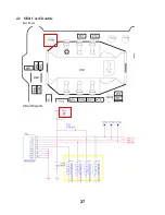
Page 37: ...37 4 2 SIM Card Trouble Test Point Circuit Diagram ...
Page 38: ...38 Checking Flow ...
Page 39: ...39 4 3 Vibrator Trouble Test Point Circuit Diagram ...
Page 40: ...40 Checking Flow NG ...
Page 41: ...41 4 4 Keypad Trouble Test Point ...
Page 42: ...42 Circuit Diagram ...
Page 43: ...43 ...
Page 44: ...44 Checking Flow ...
Page 45: ...45 4 5 RTC Trouble Test Point Circuit Diagram ...
Page 46: ...46 Checking Flow ...
Page 47: ...47 4 6 Key Backlight Trouble 4 6 1 Main Key Board LED ...
Page 48: ...48 Circuit Diagram Checking Flow ...
Page 49: ...49 4 6 2 Upper Key Board LED Circuit Diagram TP1 ...
Page 50: ...50 Checking Flow ...
Page 51: ...51 4 7 LCM Backlight Trouble Test Point Circuit Diagram ...
Page 52: ...52 Checking Flow ...
Page 53: ...53 4 8 LCM Trouble Test Point Circuit Diagram ...
Page 54: ...54 Checking Flow ...
Page 55: ...55 4 9 Microphone Trouble Test Point Circuit Diagram TP1 ...
Page 56: ...56 Checking Flow ...
Page 57: ...57 4 10 Receiver Trouble Test Point ...
Page 58: ...58 Circuit Diagram ...
Page 59: ...59 Checking Flow ...
Page 60: ...60 4 11Speaker Trouble Test Point ...
Page 61: ...61 Circuit Diagram ...
Page 62: ...62 Checking Flow ...
Page 63: ...63 4 12 Headphone Trouble Test Point Circuit Diagram ...
Page 64: ...64 ...
Page 65: ...65 Checking Flow ...
Page 66: ...66 ...
Page 67: ...67 4 13 Charging Trouble Test Point Circuit Diagram TP1 TP4 TP3 TP5 TP2 ...
Page 68: ...68 Checking Flow ...
Page 69: ...69 4 14 FM Radio Trouble Test Point ...
Page 70: ...70 Circuit Diagram ...
Page 71: ...71 Checking Flow ...
Page 72: ...72 ...
Page 74: ...74 RF Trouble TEST POINT ...
Page 76: ...76 ...
Page 77: ...77 RX Trouble TEST POINT ...
Page 78: ...78 CIRCUIT TP5 TP6 TP3 TP4 TP1 TP2 ...
Page 79: ...79 CHECKING FLOW ...
Page 80: ...80 TEST POINT CIRCUIT TP1 TP2 TP5 TP6 TP3 TP4 TP2 TP1 ...
Page 81: ...81 WAVE FORM CHECKING FLOW Replace X301 ...
Page 82: ...82 TX Trouble TEST POINT ...
Page 83: ...83 CIRCUIT WAVE FORM TP5 TP6 TP3 TP4 TP2 TP1 ...
Page 84: ...84 TEST POINT ...
Page 85: ...85 CHECKING FLOW ...
Page 86: ...86 Signal configuration CHECKING FLOW ...
Page 87: ...87 TROUBLE SHOOTING TEST POINT CIRCUIT TP5 TP6 TP3 TP4 TP1 TP2 ...
Page 88: ...88 WAVE FORM ...
Page 89: ...89 CHECKING FLOW ...
Page 90: ...90 5 DOWNLOAD 5 1 Download Setup ...
Page 100: ...100 3 DownLoad Fail If download fail that it will show red and display progress in log window ...
Page 101: ...101 Fig 2 DownLoad success DownLoad Pass will display green color ...
Page 102: ...102 6 BLOCK DIAGRAM ...
Page 103: ...103 7 CIRCUIT DIAGRMA ...
Page 104: ...104 ...
Page 105: ...105 ...
Page 106: ...106 ...
Page 107: ...107 ...
Page 108: ...108 ...
Page 109: ...109 ...
Page 110: ...110 ...
Page 111: ...111 ...
Page 112: ...112 8 BGA IC PIN Check 8 1 BGA PIN Check of MCU PMB7890 BGA use BGA non use ...
Page 113: ...113 8 2 BGA PIN Check of Memory S71GL064NA0BFW0Z0 BGA use BGA non use ...
Page 137: ...137 13 EXPLODED VIEW REPLACEMENT PART LIST 13 1 EXPLODED VIEW ...
Page 138: ...138 Ass y exploded view ...

