13
CHAPTER 2: MOTHERBOARD INFORMATION
Block Diagram
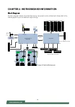
The block diagram indicates how data flows among components on the motherboard. Please refer to the
following figure for your motherboard’s layout design.
SkyLake-SP
6 Channel DDR4 RDIMM 2400 Mhz up to 320GB
PCIe x
8
PCIe x8
Intel Lewisburg PCH
(C626/C621)
BIOS
mSATA
LPC
TPM
SATAIII*5
PCIe x4
@SATA0
PCIe x8
PCIe x8 or PCIEx4*2 auto selection
SPI
PCIe x8 PCIe x8/FPGA PCIe x8/FPGA
PCIe x8
DMI*4
BIOS
Dual BIOS
U.2 connector reserved for 2U
PCIe x
1
PCIe x
1
AST-1400
AST-2400
USB 3.0x4
SFI*4
Marvell
88E1543
connector
connector
GPIO
Fan Monitor
Watchdog
Thermal Monitor
LOM/ MGNT share
port (optional)
LOM/ MGNT share
port (optional)
connector
PCIe x8 or PCIEx4*2 auto selection
NCSI with AST1400
NCSI with AST2400
Two type of IO card for different purpose
I210-AT
I210-AT
Summary of Contents for NCA-5520
Page 16: ...16...
Page 44: ...44 3 Fix the lock screws on the Ear Brackets to both front posts...
Page 63: ...63 Super IO Configuration...
Page 79: ...79 NVMe Configuration Network Stack Configuration...
Page 86: ...86 Server ME Configuration...
Page 89: ...89 Processor Configuration...
Page 91: ...91 Per Socket Configuration Feature Options Description CPU Socket0 Configuration None None...
Page 106: ...106 View System Event Log...


