Q3, U5B and CR22 produce a 1mA current source at P1 (Pin 8). The supply requires a 0
to 5 volt signal to output, zero to full current out. To get this voltage on Pin 7 (P1), the
1mA current source is conducted through a 0 to 5k Ohm pot to produce the control
voltage.
The protection circuits consist of an ignitor "time out" timer, low voltage inhibit, soft start
timer, interlock and overcurrent detector. All the protection circuits either allow Q1 to be
turned on, which turns off U7 (thus disabling the PWM) or they keep Q1 off (enabling the
PWM).
The igniter "time out" timer consists of U1B, U1A and U2. When Q1 is turned on, the
output of U1B goes high. This in turn charges C1 through R1. If this is allowed for
sufficient time, C1 will charge to a voltage greater than the 5.1V (REF) and this will cause
U1A to latch on, thus turning on Q1 and disabling the PWM. During the time that C1 is
being charged, U2 can terminate the time out by shorting C1. U2 is turned on when a
current of greater than 4 Amps is flowing from the output.
The low voltage inhibit is made up of U3A. the unregulated +12 volt supply, which
represents line voltage, is attenuated and input to U3. this input is compared to the
5.1V(REF) and turns on Q1 when the line voltage is below 180 VAC, disabling the PWM.
The soft start circuit (Q2 and U3B) turns on the soft start relay K1. Q2, which turns on the
relay, is kept biased off until C5 charges to 5.1 volts.
This takes about 10 seconds.
During these 10 seconds, the main filter capacitors' (C1) charging current is limited by the
400 Ohms of R1 for the 10 seconds, then K1 closes, shorting out the limiting resistor.
The interlock circuit is made up of CR12 & 13 and P1 (Pins 1, 9, 3 and 10). When these
pins are shorted, the input bias to Q1 is disabled, allowing the PWM to operate.
The over-current detector, U4A, monitors the voltage readback from the shunt. And, if
the voltage exceeds 5.1 volts, the output of U4A is latched high again turning on Q1,
which disables the PWM.
4.4 A200 BUCK CONVERTER
The A200 buck converter can be thought of as a switch connected between E2 and E3.
This switch, in the form of an IGBT transistor, (Q1, 2 and 3) is switched on and off at a 20
kHz rate. To get more lamp current, the switch is closed longer than normal. The choke
L2, on the main schematic, filters the chopped output, caused by the switch opening and
closing, to produce pure DC. For example, if the switch is turned on and off at a 50%
duty cycle, the output DC output voltage will be 1/2 the input DC at E1 and E2.
The switch control signal is fed to the A200 PCB from the A100 via P1. U1 is an optical
coupler to isolate the control signal. The output from U1 is amplified by U2 and fed to two
FET's which produce a bipolar drive to the transistor switches Q1, Q2 and Q3. U3
supplies the upward pull for the gate drive and U4 provides a pull down to quickly
discharge any input capacity. The output of U3 and U4 is isolated by R9 and R10 for
Q1.CR10 is a clamp diode to prevent excessive drive. Like-wise R11 and R12 are for Q2
and etc.
There are 3 switches in parallel and for this, only one will be explained. CR1 is the
flyback catch diode. CR4, CR5, C4 and R4 are snubbers to help shape the waveform
across the transistor switch for least power dissipation and voltage spikes. The chokes
L1A, B and C are for balancing the current between the switch transistors. C10, C1, C2
and C3 are filters for the 20 kHz switching signals.
Page 14 of 18
83-475-001 Rev. D
Summary of Contents for ESKI
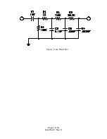
Page 6: ...Figure 1 Loss Pass Filter Page 4 of 18 83 475 001 Rev D...
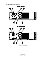
Page 8: ...3 OPERATING INSTRUCTIONS Figure 2 Front Panels Page 6 of 18 83 475 001 Rev D...
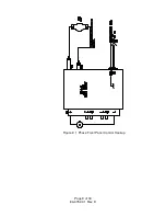
Page 11: ...Figure 3 1 Phase Front Panel Control Hookup Page 9 of 18 83 475 001 Rev D...
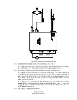
Page 14: ...Figure 4A 1 Phase External Control Hookup Page 12 of 18 83 475 001 Rev D...

