3.1
Frequency Configuration
Chapter 3 Electrocircuit
The transmitter signal is generated by the
3.2 Receiver Elements (RX)
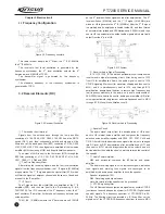
Figure 3.3 Frequency structure
nd
st
This radio receiver adopts the 2 Mixer, the 1 IF 51.65MHz,
nd
the 2 IF 450kHz.
The receiver's first local oscillation is generated by the
nd
th
frequency synthesizer, the 2 local oscillation selects the 4
harmonic wave 51.2MHZ of TCXO.
frequency
synthesizer.
The standard frequency of the frequency synthesizer is
generated by TCXO.
Figure 3.4 Receiver Illustration
Figure 3.5 IF System
The receiver front terminal
Signals from the antenna pass through the low pass filter
consisting of L104, C546, L103, C545, L102, C534 and the RX/TX
switch (D51); and then undesirable out-of-band signals will be
filtered out at the band pass filter (BPF) consisting of L104, C546,
L103, C545, L102, C534; then signals are amplified at the low noise
amplifier (LNA) consisting of Q81 and its peripheral components.
The output of LNA is sent to the first mixer (Q79) through the
BPF filter consisting of L115, C541, D63, C528, C591, L114, D62,
C527, C590, L113, D60 and C526.
The First Frequency Mixer
After mixing the receiving signals and the first local oscillation
st
signals from the frequency synthesizer, the 1 IF signals (51.65MHz)
st
are generated. The 1 IF signals pass the crystal filter (XF2), which
will filter the signals of adjacent channel and those out of band, and
are sent to the IF amplifier.
IF Circuit
st
The IF signals from the crystal filter are amplified at the 1 IF
amplifier (Q78), and then are sent to the IF processing IC (U9,
nd
nd
TA31136FN). The IF IC consists of the 2 frequency mixer, the 2
local oscillator, IF amplifier, limiter, phase frequency detector, and
noise amplifier.
th
TCXO (X4, 12.8MHz) selects the 4 harmonic wave 51.2MHZ
nd
nd
as the 2 local oscillation signal source after amplification. The 2
st
local oscillation (51.2MHz) and the 1 IF signal (51.65MHz) are
nd
nd
mixed at U9 to generate the 2 IF (450MHz). After the 2 IF signal
is amplified and its amplitude is limited inside U9, and then filtered
at porcelain filter (wideband CF4/Nattowband 3, 450kHz) and then
sent to U9 to demodulate the output audio signals which are finally
th
output from the 9 pin of U9.
Receiver Audio Signal Processing
IC13, IC12, IC16, IC15 and their peripheral circuit compose the
receiver audio signal processing circuit. After being sent to IC13
from U9 for amplification Audio, the audio signal is sent to IC15
CTCSS signaling filter circuit for waveform shaping and then sent to
MCU; and it is simultaneously sent to IC12 and through IC12
amplification, deemphasis, filtration to remove high frequency and
low frequency elements in the audio, only audio components of
300--3000Hz are kept to be sent to audio power amplifier (U9) after
volume potentiometer adjustment, and simultaneously sent to MCU
through IC15 (2 tone/5 tone filtration circuit).
Squelch Circuit
The audio signal output from the demodulation of U9 is sent
back to U9 internal noise amplifier and composes the frequency
selection noise amplifier together with C320, Q77, R167, C439 and
C319. Filtered from the demodulation signals, the noise is changed
into DC level by D57 demodulation after amplification by Q77 and
then sent to MCU, which distinguishes the noise volume so as to
decide whether to enable the squelch, which achieves the control of
the squelch.
Audio Power Amplifier
Q92 and peripheral compose the BTL-audio and power
amplifier.
The audio receiving signals, voice indication signals, indication
tone signals and warning tone signals are converged to be
amplified by the audio power amplifier to drive the speaker.
Speaker impedance:
16Ù
Q95: Receiving audio signal switch
Note: No terminal of the speaker can be grounded!
CTCSS signaling filter
The U9 Demodulation output audio signals may contain CTCSS
(continuous tone coded squelch system) or DCTCSS (Digital coded
squelch) signals. The frequency spectrum of CTCSS/DCS is 20-
250Hz. The filtering circuit constructed by IC16can filter out the
signals out of the CTCSS/DCS frequency spectrum to ensure MCU
Figure 3.6 Receiver Audio Processing
PT7200 SERVICE MANUAL
2
Summary of Contents for PT7200-01
Page 1: ...PROFESSIONAL TWO WAY RADIO PT7200 V071215 FM PORTABLE RADIO SERVICE MANUAL ...
Page 29: ...Figure 1 PT7200 Top Board Position Mark Diagram 136 174 ...
Page 30: ......
Page 31: ...Figure 1 PT7200 Top Board Position Mark Diagram 400 470 ...
Page 32: ......
Page 35: ...Figure 7 Schematic Circuit Pane Diagram PT7200 SERVICE MANUAL 26 33 ...


