


Keysight M8132A 640 GSa/s Digital Signal Processor User’s Guide
91
Remote Programming
6
Description
The command sets both multiplexers’ registers, except the Clear Bits,
which are handled in a separate command. The Reset value in hardware
for both registers is 0, meaning:
• Input Mux: Control Input Pin 0 is mapped to all Mux outputs.
• Output Mux: FPGA Trigger Out Pin 0 is mapped to all Mux outputs.
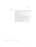
Further mappings are provided in the following tables:
Table 15
Mapping between input and output ports of the Input Multiplexer
Table 16
Mapping between input and output ports of the Output Multiplexer
Value (binary)
Port
0000
Control In (0)
0001
Control In (1)
0010
Control In (2)
0011
Control In (3)
0100
Control In (4)
0101
Trig In
0110
Reserved, do not use
0111
Reserved, do not use
1000
LOOP_BACK (0)
1001
LOOP_BACK (1)
Value (binary)
Port
000
GP_TRIG_OUT_A(0)
001
GP_TRIG_OUT_A(1)
010
GP_TRIG_OUT_A(2)
011
GP_TRIG_OUT_B(0)
100
GP_TRIG_OUT_B(1)
101
GP_TRIG_OUT_B(2)