DP-1100B II
2. IC OPERATION OF EACH CIRCUIT AND PIN DESCRIPTION
Pin No.
Symbol
I/O
Waveform
Description
Remarks
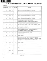
60
DSLP
0
/ 1 3 8 ^ S \
5
v
( 50
nS
—-y
0 V
Data status signal output. (Error information signal output)
63
DAST
0
V I i i 11 11/ o V
138
nS
Data status signal output. (Error information signal output)
64
D I V -
0
138
ixS
Buffer memory status output.
Outputs an " H " signal when the jitter absorption buffer memory
enters range of + 2 or + 3 frames in its capacity of ± 4 frames.
This output is connected to pin DIV- of TC9178F (IC8) to lower the
disc motor revolution.
Connected to DIV —
(pin 5) of TC9178F
(IC8)
65
DIV +
0
138
nS
Buffer memory status output.
Outputs an " H " signal when the jitter absorption buffer memory
enters range of —2 or —3 frames in its capacity of ± 4 frames.
This output is connected to pin D I V + of TC9178F (IC8) to raise the
disc motor revolution.
Connected to DIV +
(pin 4) of TC9178F
(IC8)
66
BUSE
1
Buffer selection input pin.
Selects the output condition of DIV —/DIV + .
At " H " , D i v ± output are made when the buffer memory enters
range of ± 2 frames. |At " L " , D i v ± output are made when it enters
66
BUSE
1
range of ± 3 framesj
T a b l e 2 - 3 - 4 A
96
Summary of Contents for DP-1100 B
Page 3: ...D P 1 1 0 0 B II D P 1 1 0 0 B II I BLOCK DIAGRAM ...
Page 32: ...D P 1 1 0 0 B II 1 CIRCUIT DESCRIPTION Disc Scratch Dust RFES D C O N D O C K Fig 1 2A 3 5 ...
Page 112: ...2 IC OPERATION OF EACH CIRCUIT AND D P 1 1 0 0 B II PIN DESCRIPTION Fig 2 4 1 G 1 ...
Page 117: ...DP 1100B II I OPERATION OF MAIN MICROPROCESSOR Fig 3 1D Q data reading flow chart ...


