DP-IIDOB/n
2. IC OPERATION OF EACH CIRCUIT AND PIN DESCRIPTION
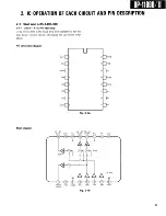
Pin description of I C 1 5 ( T M P 4 7 4 0 N )
Pin No.
Port name
Signal
name
IN/OUT Level
Function/operation
1
R4
R40
MDO
0
L
Outputs various mode data and kick data outputs to IC15 (TC15G008AP) for interface with
the servo system.
2
R4
R41
MD1
0
L
Outputs various mode data and kick data outputs to IC15 (TC15G008AP) for interface with
the servo system.
3
R4
R42
MD2
0
L
Outputs various mode data and kick data outputs to IC15 (TC15G008AP) for interface with
the servo system.
4
R4
R43
MD3
0
L
Outputs various mode data and kick data outputs to IC15 (TC15G008AP) for interface with
the servo system.
5
R5
R50
MD4
0
L
Data select signal output to ICI 5 (TC15G008AP). (The kick control data at " H " level and
the mode control data at " L " level.)
6
R5
R51
SVCS
l/N
L
Operation start/stop control signal to the servo control microprocessor IC12 (MB88201)
7
R5
R52
A2
0
L
Address data output to the external RAM IC14 (TC-5514P).
8
R5
R53
A1
0
L
Address data output to the external RAM IC14 (TC-5514P).
9
R6
R60
AO
0
H
Address data output to the external RAM IC14 (TC-5514P).
10
R6
R61
A3
0
H
Address data output to the external RAM IC14 (TC-5514P).
11
R6
R62
A4
0
H
Address data output to the external RAM IC14 (TC-5514P).
12
R6
R63
A5
0
H
Address data output to the external RAM IC14 (TC-5514P)
13
R7
R70
DO/QDAd
I/O
H
1 Data input terminal of the subcode Q from IC8 (TC-9178), (T-6391).
2 Data input/output terminal.with the external RAM IC14 (TC5514).
14
R7
R71
D1/QDAC
I/O
H
1 Data input terminal of the subcode Q from IC8 (TC-9178), (T-6391).
2 Data input/output terminal with the external RAM IC14 (TC5514).
15
R7
R72
D2/QDAD
I/O
H
1 Data input terminal of the subcode Q from IC8 (TC-9178), (T-6391).
2 Data input/output terminal with the external RAM ICI 4 (TC5514).
16
R7
R73
D3/QDAa
I/O
H
1 Data input terminal of the subcode Q from IC8 (TC-9178), (T-6391).
2 Data input/output terminal with the external RAM IC14 (TC5514).
17
P1
P10
A6
0
H
Address data to the external RAM IC14 (TC5514).
18
P1
P11
A7
0
H
Address data to the external RAM IC14 (TC5514).
19
P1
P12
A8
0
H
Address data to the external RAM IC14 (TC5514).
20
P1
P13
A9
0
H
Address data to the external RAM IC14 (TC5514).
T a b l e 2 - 3 - 1 A
75
Summary of Contents for DP-1100 B
Page 3: ...D P 1 1 0 0 B II D P 1 1 0 0 B II I BLOCK DIAGRAM ...
Page 32: ...D P 1 1 0 0 B II 1 CIRCUIT DESCRIPTION Disc Scratch Dust RFES D C O N D O C K Fig 1 2A 3 5 ...
Page 112: ...2 IC OPERATION OF EACH CIRCUIT AND D P 1 1 0 0 B II PIN DESCRIPTION Fig 2 4 1 G 1 ...
Page 117: ...DP 1100B II I OPERATION OF MAIN MICROPROCESSOR Fig 3 1D Q data reading flow chart ...


