background image

XV-LTR1

1-7

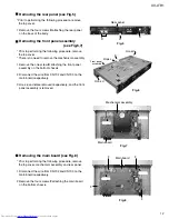
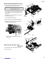
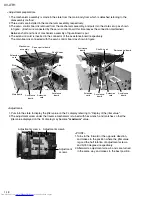
Removing the rear panel (see Fig.5)

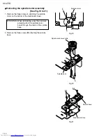
Removing the front panel assembly
                                                (see Fig.6,7)

Removing the main board (see Fig.8)

*Prior to performing the following procedure, remove
  the top cover.

1.Remove the four screws 

D

 attaching the rear panel

   on the back of the body.

* Prior to performing the following procedure, remove
  the top cover.
* There is no need to remove the mechanism assembly.

1.Remove the one screw 

E

 attaching the front panel

   assembly on the bottom chassis.

2.Disconnect the wire from CN702 and CN703 on the
   main board respectively.

3.Hook 

c

 and 

d

 are removed respectively, and the front

   panel assembly is removed. 

* Prior to performing the following procedure, remove
  the top cover, mechanism assembly and rear panel.

1.Disconnect the wire from CN702 and CN703 on the
   main board respectively.

2.Remove the four screws 

F

 attaching the main board

   on the bottom chassis.

D

D

D

Rear panel

Fig.5

E

Hook c

Hook d

Hook d

Front panel

assembly

Fig.6

CN703

CN702

Fig.7

Main board

Mechanism assembly

CN703

CN702

Fig.8

F

F

F

F

Main board

Summary of Contents for XV-LTR1

Page 1: ...Area Suffix J U S A This service manual is printed on 100 recycled paper Contents Safety precautions 1 2 Preventing static electricity 1 3 Importance admistering point on the safety 1 4 Precautions for service 1 5 Disassembly method 1 6 Adjustment method 1 15 Troubleshooting 1 19 Description of major ICs 1 23 ...

Page 2: ...t screw heads headphone jack control shafts etc to be sure the product is safe to operate without danger of electrical shock Do not use a line isolation transformer during this check Plug the AC line cord directly into the AC outlet Using a Leakage Current Tester measure the leakage current from each exposed metal parts of the cabinet particularly any exposed metal part having a return path to the...

Page 3: ...ing transport and before installation both sides of the laser diode on the replacement optical pickup are shorted After replacement return the shorted parts to their original condition Refer to the text 2 Do not use a tester to check the condition of the laser diode in the optical pickup The tester s internal power source can easily destroy the laser diode 1 2 Handling the traverse unit optical pi...

Page 4: ...2 B7139 B7123 B7502 B7607 B7207 C11 C12 C13 C14 C15 C16 C1701 C1702 C17 C421 C422 C609 C619 C629 C649 C659 C701 C707 C711 C714 C716 C717 C718 C728 C730 C731 C740 C741 C742 C744 C745 C746 C747 C750 C751 C752 C754 C755 C756 C757 C761 C762 C771 C772 C821 C902 C907 C914 C918 C960 C962 C963 C964 C965 C966 C969 C973 C978 C979 C982 C984 C985 C987 C989 C992 C995 C996 C997 CN701 CN702 CN703 CP951 CP952 D60...

Page 5: ...he optical block Do not change the setting of these half fixed resistors for laser power adjustment Destruction of Traverse Unit and Laser Pickup by Static Electricity Laser diodes are easily destroyed by static electricity charged on clothing or the human body Before repairing peripheral elements of the traverse unit or pickup be sure to take the following electrostatic protection 1 Wear an antis...

Page 6: ...ontrol board is removed from the connector CN961 and CN701 connected with the main board respectively 4 Remove the mechanism assembly by lifting the rear part of the mechanism assembly Prior to performing the following procedure remove the top cover and mechanism assembly 1 Disconnect the card wire from connector CN201 and CN202 on the servo control board respectively 2 Disconnect the flexible wir...

Page 7: ...aching the front panel assembly on the bottom chassis 2 Disconnect the wire from CN702 and CN703 on the main board respectively 3 Hook c and d are removed respectively and the front panel assembly is removed Prior to performing the following procedure remove the top cover mechanism assembly and rear panel 1 Disconnect the wire from CN702 and CN703 on the main board respectively 2 Remove the four s...

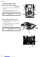
Page 8: ...owing procedure remove the clamper assembly Push b of the slide cam into the slot on the left side of the loading base until it stops Draw out the tray toward the front 1 2 Removing the tray See Fig 2 and 3 When reattaching fit the clamper to the two joints a ATTENTION Before reattaching the tray slide the part c of the slide cam to the right as shown in Fig 3 ATTENTION Joint a Joint a A A A A Fig...

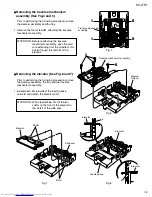
Page 9: ...evator ATTENTION Prior to performing the following procedure remove the clamper assembly the tray and the traverse mechanism assembly Extend each bar e inside of the loading base outward and detach the elevator shaft 1 Removing the elevator See Fig 6 and 7 When reattaching first fit the two shafts on the front of the elevator to the slots f of the slide cam ATTENTION Fig 4 Fig 5 Fig 6 Fig 7 B B B ...

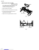
Page 10: ...e elevator Remove the belt from the pulley Remove the screw C attaching the motor assembly Turn over the body and remove the screw D attaching the motor assembly Release the two tabs g retaining the motor board 1 2 3 4 Removing the motor assembly See Fig 8 and 9 Fig 8 Fig 9 C Motor assembly Belt Loading base Motor assembly D Tabs g ...

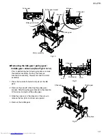
Page 11: ... gear bracket in the direction of the arrow and pull out the pulley gear Slide the slide cam in the direction of the arrow to release the two joints i and remove upward Remove the middle gear 1 2 3 4 Removing the Idle gear pulley gear middle gear slide cam See Fig 10 to 12 Fig 11 Fig 12 Fig 10 Motor assembly Pulley gear Pulley gear bracket Pulley gear bracket E Idle gear Idle gear Pulley gear Tads...

Page 12: ...g make sure that the thrust spring presses the feed gear M and the feed gear E reasonably ATTENTION Remove the feed gear M Pull out the feed gear E and the lead screw Remove the two screws H attaching the feed motor 2 3 4 When reattaching pass the two cables extending from the feed motor through the notch k of the feed holder as shown in Fig 13 ATTENTION Traverse mechanism assembly section Fig 13 ...

Page 13: ...e the part m in the direction of the arrow and detach from the spindle base Disengage the joint n of the pickup and the shaft in the direction of the arrow Pull out the shaft from the pickup Remove the two screws J attaching the actuator Disengage the joint of the actuator and the lead spring Pull out the lead spring 2 3 4 5 6 The spring must be under the shaft when you install pick up Fig 16 Fig ...

Page 14: ...ndle motor assembly See Fig 19 to 21 When reattaching pass the card wire extending from the spindle motor board through the notch of the spindle base ATTENTION Remove the three screws M attaching the spindle base 2 Fig 19 Fig 20 Fig 21 Spindle motor assembly Spindle base L M M Spindle base Mechanism base L L Spindle motor ...

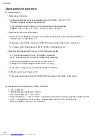
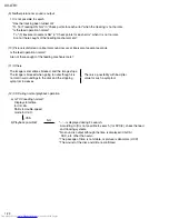
Page 15: ...6 Press the PLAY button 7 The laser current value and the jitter value is displayed on the FL indicator as follows Laser current value and Jitter value are displayed on the FL display by the undermentioned method Please refer to the failure diagnosis 0 0 4 0 3 9 7 8 FL Display Laser current value Jitter value The test mode is canceled when the power is turned off The laser current value becomes 40...

Page 16: ...areful check it if there is neither damage nor dirt on the read surface For Jitter value When you exchange the pick up When you exchange the spindle motor When the reading accuracy of the signal is bad There is a block noise in the screen etc In the following cases please adjustment 3D PHONIC Button Initialize start POWER Button DTS Display part Initialize complete FL Display OPEN CLOSE Button Tes...

Page 17: ...IN CONNECT EXTXVS40MK2CB 1 MAIN CONNECT Parts No EXTXVS40MK2CB Parts No EXTXVS40CB Parts No EXTXV521CB These parts are not used CN501 XV 521 CN706 XV 521 MAIN CONNECT XV 521 CN502 CONT CONNECT CN701 XV 521 MAIN CONNECT CONT CONNECT XV 521 CN601 MAIN CONNECT XV 521 CN503 CONT CONNECT XV 521 CN601 MAIN CONNECT XV 521 CN503 CONT CONNECT Hex wrench for adjustment Off the shelf 1 3mm Test disc VT 501 o...

Page 18: ... figure 1 Puts into the state to display the jitter value on the FL display referring to Display of the jitter value 2 The adjustment screw under the traverse mechanism is turned with hex wrench and matches so that the jitter value displayed on the FL display may become maximum value Adjustment screw a Adjustment screw b Adjustment screw c POINT 1 Turns in the forward or the opposite direction and...

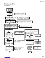
Page 19: ...everal seconds and becomes NO DISC or an error display afterwards The rotation of DISC becomes high speed and abnormal and becomes NO DISC or an error display afterwards Is focus retraction OK Even when it retracts correctly if it is out of focus and makes repeated retries with a clicking sound it is in error Is tracking retraction OK If TE waveform reappears or fails to converge after the TE retr...

Page 20: ...or 3 Has the control signal come from servo IC or the microcomputer Is it L while the terminal of IC251 18 SBRK is operating Is it H while the terminal of IC251 23 SPMUTE is operating Is the control signal input to the terminal of IC251 22 EC changes from VHALF voltage while the motor is working Is the VHALF voltage input to the terminal of IC251 21 ECR 4 Is the FG signal input to the servo IC Is ...

Page 21: ...racking been turned on Spindle motor and driver is defective Additionally IC101 and IC301 and Mechanism is defective jitter etc are thought Besides the undermentioned cause is thought though specific of the cause is difficult because various factors are thought Mechanism is defective jitter IC301 IC401 The disc is dirty or the wound has adhered 7 Address read NG 8 Between layers jump NG double lay...

Page 22: ...echanism etc The image is sometimes blocked and the image stops The image is blocked when going to outer though it is normal in surroundings in the disk and the stopping symptom increases There is a possibility with bad jitter value for such a symptom 12 CD During normal playback operation a Is TOC reading normal Displays total time for CD DA Shifts to double speed mode for V CD b Playback possibl...

Page 23: ...ymbol LPC1 LPC01 LPC2 LPC02 VFOSHORT TBAL FBAL POFLT DTRD IDGT STANDBY SEN SCK STDI RSCL JLINE TEN TEOUT AGCBAL ASOUT FEN FEOUT AGCOFST MON AGCLVL GND2 VREF2 VCC2 VHALF DFLTON DFLTOP DCFLT GND3 I O Description Pin No Symbol I O Description 34 35 36 37 38 39 40 41 42 43 44 45 46 47 48 49 50 51 52 53 54 55 56 57 58 59 60 61 62 63 64 RFDIFO RFOUT VCC3 RFC DCRF OFTR BDO RFENV BOTTOM PEAK AGCG AGCO TES...

Page 24: ...O O O O I O I I O I I Non inverted output of CH4 Inverted output of CH4 Non inverted output of CH3 Inverted output of CH3 Vcc for CH3 4 power block Input for Ch4 stand by control Substrate ground Output for CH3 OP AMP Inverting input for CH3 OP AMP Non inverting input for CH3 OP AMP Output for CH4 OP AMP Inverting input for CH4 OP AMP Non inverting input for CH4 OP AMP Vcc for pre block 1 Block di...

Page 25: ...K Q ECR EC PS FG VCC Vcc VCC GSW VM RNF RNF VM GAIN SWITCH 2 4 7 8 9 10 11 12 13 14 Hall 1 Hall 2 Hall 3 H1 H1 H2 H2 H3 H3 SERVO SIGNAL TSD PS TOROUE SENSE AMP CURRENT SENSE AMP GAIN CONTROL DRIVER HALL AMP TL A3 A2 A1 GND NC A3 NC A2 NC NC A1 GND H1 H1 H2 H2 H3 H3 RNF VM GSW Vcc FG PS EC ECR FR FG2 SB CNF BR VH 1 2 3 4 5 6 7 8 9 10 11 12 13 14 28 27 26 25 24 23 22 21 20 19 18 17 16 15 29 30 ...

Page 26: ...ut for hall input AMP 2 Positive input for hall input AMP 3 Negative input for hall input AMP 3 Hall bias terminal Non connect Capacitor connection pin for phase compensation Short brake terminal Non connect Non connect Torque control standard voltage input terminal Torque control voltage input terminal Start stop switch power save terminal FG signal output terminal Power supply for signal divisio...

Page 27: ... DQ4 Vcc Q DQ5 DQ6 V SSQ DQ7 Vcc LDQM WE CAS RAS CS BS0 BS1 A10 AP A0 A1 A2 A3 Vcc V SS DQ15 V SSQ DQ14 DQ13 Vcc Q DQ12 DQ11 V SSQ DQ10 DQ9 Vcc Q DQ8 V SS N C UDQM CLK CKE NC A11 A9 A8 A7 A6 A5 A4 V SS 1 2 3 4 5 6 7 8 9 10 11 12 13 14 15 16 17 18 19 20 21 22 23 24 25 26 27 54 53 52 51 50 49 48 47 46 45 44 43 42 41 40 39 38 37 36 35 34 33 32 31 30 29 28 Symbol CLK CS CKE A0 A11 BS0 1 RAS CAS WE LDQ...

Page 28: ... power NTSC PAL switch input RGB YC Switch input S COMPONENT Switch input Key input S831 S835 Key input open close Not used Not used Power supply B 5V RGB select control H RGB L other Reset input AV COMPULINK output AV COMPULINK input Power ON output Tray close control output Tray open control output Tray muting output L muting Detection switch of tray open close L open close Detection switch of t...

Page 29: ...4 55 56 57 58 59 60 61 62 63 64 65 66 67 68 69 70 71 72 73 74 75 76 77 78 79 80 81 82 83 84 85 86 87 88 89 90 91 92 93 94 95 96 97 98 99 100 P85 TM5IO VDD FEPEN SLEEP BUSY REQ VSS EPCS EPSK EPDI EPDO VDD SCLKO S2UDT U2SDT CPSCK P74 SBI1 SDOUT NMI ADSCIRQ ODCIRQ DECIRQ CSSIRQ ODCIRQ2 ADSEP RST VDD TEST1 TEST2 TEST3 TEST4 TEST5 TEST6 TEST7 TEST8 VSS D0 D1 D2 D3 D4 D5 D6 D7 Connect to TP406 Connect t...

Page 30: ...ymbol NINT0 1 VDD3 VSS NINT2 WAITDOC NMPST DASPST CPUADR17 9 VDD18 VSS DRAMVDD18 DRAMVSS CPUADR8 0 VDD3 VSS DRAMVDD3 NCS NWR I O Description 3 Pin function 1 4 Interruption of system control 0 1 Power supply terminal for I O 3 3V Connect to ground Interruption of system control 2 Wait control of system control Reset of system control Non connect Setting of initial value of DASP signal System contr...

Page 31: ...ck signal input Drop out signal input Non connect Power supply terminal for I O 3 3V Power supply terminal for DRAM 1 8V Connect to ground for DRAM Connect to ground Non connect Tracking balance adjustment output Focus balance adjustment output Traverse drive output Spindle drive output Motor FG input Non connect Non connect Non connect Digital output signal Non connect Non connect Power supply te...

Page 32: ...nect to capacitor 2 1 for DSL Power supply terminal for analog circuit 3 3V Equivalence RF Equivalence RF Output for jitter signal monitor Connect to ground for analog circuit Tracking drive output Focus drive output Power supply terminal for analog circuit 3 3V Focus error input Phase difference 3 beams tracking error AS Full adder signal RF envelope input DVD laser current control terminal CD la...

Page 33: ...ct to ground ATAPI host data 6 8 Reference power supply for ATAPI 5 0V ATAPI host reset input ATAPI master slave select 1 2 3 4 5 6 7 CLR1 D1 CK1 PR1 Q1 Q1 GND 14 13 12 11 10 9 8 Vcc CLR2 D2 CK2 PR2 Q2 Q2 CK1 D1 Q1 Q1 PR1CLR1 CK2 D2 Q2 Q2 PR2CLR2 74VHC74MTC X IC454 ZIVA Wait 1 Terminal layout 3 Pin function 2 Trouth table CLR L H L H H H PR H L L H H H D X X X L H X CK X X X Q L H H Note 1 L H Qn ...

Page 34: ...Input Output GND CY24203SC X IC571 MPEG Audio clock generator with VCXO 1 2 3 4 8 7 6 5 XIN VDD VCXO VSS XOUT 27M 13 5M 16 9344M 1 2 3 4 5 6 7 8 XIN VDD VCXO VSS 16 9344M 13 5 27M XOUT Reference crystal input Power supply Input analog control for VCXO Connect to ground 16 9344 MHz clock output 13 5 MHz clock output 27 MHz clock output Reference crystal output Pin No Description Symbol 1 Pin layout...

Page 35: ... DAC Power supply terminal Non connect Connect to ground Control signal for DAC Control signal for DAC Analog output 1 Power supply terminal Analog output 1 Connect to ground Connect to ground Analog output 2 Power supply terminal Analog output 2 Control signal for DAC Connect to ground Non connect Non connect VCO Frequency Power supply D 5V Connect to ground Connect to ground Control signal for D...

Page 36: ...in the state of high impedance Address Buffer A0 A1 A2 A3 A4 A5 A6 A7 A8 A9 A10 A11 A12 A13 A14 A15 A16 A17 A18 A19 A20 Symbol A0 A20 D0 D14 CE OE BYTE Vcc Vss WE WP Function Address Input Data Output Chip Enable Output Enable Mode Switch Power Supply GND Write enable Connect to ground 3 Pin functions WP A20 A9 A10 A11 A12 A13 A14 A15 A16 A17 BYTE Vss A0 D7 D14 D6 D13 D5 D12 D4 Vcc 1 2 3 4 5 6 7 8...

Page 37: ... X IC741 IC751 Dual OP amplifier Block diagram 1 2 3 INPUT OUTPUT GND NJM78M05FA IC953 Regulator 1 INPUT 2 GND 3 OUTPUT 1 Terminal layout 2 Block diagram 2 Block diagram 1 Terminal layout PQ05RD21 IC951 Regulator PQ05RD21 Vin Vout GND Vcontrol 2 1 3 4 Vcontrol Voutput Vinput GND ...

Page 38: ...function 1 2 3 4 8 7 6 5 PE VCC CS SK NC GND DO DI 1 2 3 4 5 6 7 8 PE VCC CS SK DI DO GND NC Non connect Power supply terminal Chip select input Serial clock input Serial data input Serial data output Connect to ground Non connect Pin No Description Symbol I I I O I O D 2 1 S 5 3 O C P F B GND Comp 2 4 VIN START REG T S D O V P LATCH O S C Vth 2 DRIVE Comp 1 Vth 1 STR G6651 IC901 Switch regulator ...

Page 39: ...ly 3 3V Video data bus output Byte serial CbYCrY data synchronous with VCLK Video data bus output Byte serial CbYCrY data synchronous with VCLK Video data bus output Byte serial CbYCrY data synchronous with VCLK Video data bus output Byte serial CbYCrY data synchronous with VCLK Video data bus output Byte serial CbYCrY data synchronous with VCLK Video data bus output Byte serial CbYCrY data synchr...

Page 40: ...n connect Non connect Non connect Programmable I O terminal Connect to ground Power supply terminal 3 3V Programmable I O terminal Programmable I O terminal Programmable I O terminal Programmable I O terminal Programmable I O terminal Programmable I O terminal Programmable I O terminal SDRAM data SDRAM data Power supply terminal 3 3V Connect to ground SDRAM data SDRAM data SDRAM data SDRAM data SD...

Page 41: ...r SDRAM SDRAM bank select SDRAM address SDRAM address Power supply terminal 3 3V Connect to ground SDRAM address SDRAM address SDRAM address Tie to VSS or VDD_3 3 as specified in table1 Non connect Non connect Tie to VSS or VDD_3 3 as specified in table1 Non connect Tie to VSS or VDD_3 3 as specified in table1 Tie to VSS or VDD_3 3 as specified in table1 Tie to VSS or VDD_3 3 as specified in table...

Page 42: ...deo DAC video output format Macrovision encoded Power supply terminal for analog video DAC Power supply terminal for analog video Non connect Connect to ground for analog video DAC Connect to ground for analog video DAC video output format Macrovision encoded Power supply terminal for analog video DAC Power supply terminal for analog video Connect to ground for analog video Reference resistor Conn...

Page 43: ...erface registers Host addressbus 3 bit address bus selects one of eight host interface registers Tie to VSS or VDD_3 3 as specified in table 1 Tie to VSS or VDD_3 3 as specified in table 1 Tie to VSS or VDD_3 3 as specified in table 1 Connect to ground Power supply terminal 2 5V Tie to VSS or VDD_3 3 as specified in table 1 Connect to ground Power supply terminal 3 3V Tie to VSS or VDD_3 3 as spec...

Page 44: ...Printed in Japan 200111 S No A0020 XV LTR1 VICTOR COMPANY OF JAPAN LIMITED PERSONAL MOBILE NETWORK BUSINESS UNIT 1644 Shimotsuruma Yamato Kanagawa 242 8514 Japan ...

Page 45: ...le as service parts XV LTR1 Contents Exploded view of general assembly and parts list DVD Traverse mechanism assembly and parts list DVD Loading mechanism assembly and parts list Electrical parts list Packing materials and accessories parts list 3 2 3 4 3 6 3 8 3 14 Area Suffix J U S A ...

Page 46: ... B E C B D C D 6 5 7 7 9 11 11 35 31 16 24 Main Board 15 13 14 3 3 14 34 32 33 33 10 1 4 2 12 11 8 30 23 39 30 22 36 37 37 37 38 38 30 20 28 26 29 29 25 27 29 29 20 19 20 20 21 21 21 21 Exploded view of general assembly and parts list Block No M M M 1 16 16 16 ...

Page 47: ... SPACER 2 15 LE40768 002A PROTECT SHEET 1 16 QYSBSGG3008E T SCREW 4 19 DVD TRAVERSE MECHANISM 1 20 LV41659 201A INSULATOR 4 21 LV41424 001A SPECIAL SCREW 4 22 DVD LAODING MECHANISM See page 3 4 See page 3 6 1 23 LV10455 002A TRAY 1 24 LV20913 002A CLAMPER BASE 1 25 LV32417 001A CLAMPER 1 26 LV42089 001A YOKE 1 27 LV41118 003A MAGNET 1 28 LV41741 001A SPECIAL SCREW 1 29 QYSBSF2008Z SCREW 4 30 QYSBS...

Page 48: ...6 013B PG 641 CFD 4007ZY2 12 0mm 0 2mm 65 2mm mm 0 0 2 10 26 24 25 15 17 14 21 21 19 20 18 22 27 16 16 28 3 3 2 13 13 6 5 4 9 8 11 12 7 1 29 30 30 30 29 29 23 3 7 DVD Traverse mechanism assembly and parts list Block No M M M 2 ...

Page 49: ...10 LV41511 002A FEED GEAR 1 11 LE40742 001A TORSION SPRING 1 12 QYSDSF2005Z SCREW 1 13 QYSDST2605M TAPPING SCREW 2 14 LE20517 001A HOLDER 1 15 LE40744 001A SPRING 1 16 LV41121 002A SLIDE SHAFT 2 17 QYSDST2605M TAPPING SCREW 1 18 QAL0342 001 OPTICAL PICK UP 1 19 LE20519 001A ACTUATOR 1 20 LE30886 001A SPRING 1 21 QYSPSFU1740Z SCREW 2 22 LE30888 003A SPRING 1 23 QYSPSGU1430Z SCREW 1 24 LE40743 001A ...

Page 50: ...XV LTR1 3 6 A A 6 85mm 0 1mm 13 12 10 9 8 3 2 5 14 4 1 11 7 6 DVD Loading mechanism assembly and parts list Block No M M M 3 Grease UD 24H2 EM 30L CFD 4007ZY2 2 3 ...

Page 51: ...77 003 MINI SCREW 1 6 LV42209 001A BELT 1 7 LV42084 002A PULLEYGEAR 1 8 LV42085 002A MIDDLE GEAR 1 9 LV42086 001A IDLE GEAR 1 10 LV32514 002A SLIDE CAM 1 11 LV42348 001A GEAR BRACKET 1 12 QYSBSF2006Z SCREW 1 13 LV20912 002A ELEVATOR 1 14 QUQ110 0610AJ FFC WIRE 1 Electrical parts list Loading motor board Block No 03 Item Parts number Parts name Area Remarks A CN 1 S 1 S 2 QGF1016F3 06 QSW0910 002 Q...

Page 52: ...TN1CM 107Z E CAPACITOR 100MF 20 16V C 772 QETN1CM 107Z E CAPACITOR 100MF 20 16V C 797 NCB31HK 152X C CAPACITOR C 801 NCB31CK 104X C CAPACITOR C 802 QEKC1AM 476Z E CAPACITOR 47MF 20 10V C 821 QEKC1HM 475Z E CAPACITOR 4 7MF 20 50V C 902 QFZ9075 683 M CAPACITOR A 068MF C 906 QCZ9079 102 C CAPACITOR A 1000PF C 907 QETM2DM 157 E CAPACITOR A 150MF 20 C 908 NZZ000000000500 C CAPACITOR C 909 NZZ0000000004...

Page 53: ... I M Q 631 KTA1267 G T TR I M Q 743 2SD2144S VW T TRANSISTOR AMUTE1 Q 753 2SD2144S VW T TRANSISTOR AMUTE1 Q 791 KRA102S X DIGITAL TR Q 951 KTD863 Y T TRANSISTOR Q 952 KRA104S X DIGITAL TR Q 953 KTA1267 G T TR I M Q 964 2SB1184 QR X TRANSISTOR A Q 965 KTC3199 Y T TR I M Q 966 KTA1267 G T TR I M Q 991 KTC3199 Y T TR I M R 1 NRSA63J 910X MG RESISTOR R 20 NRSA63J 271X MG RESISTOR R 25 NRSA63J 100X MG ...

Page 54: ... OMF RESISTOR 68K 5 1 2W R 906 QRE141J 681Y C RESISTOR 680 5 1 4W R 907 QRT022J R47 OMF RESISTOR 5 1 2W R 908 QRE141J 332Y C RESISTOR 3 3K 5 1 4W R 910 QRE141J 754Y C RESISTOR 750K 5 1 4W R 911 QRE141J 754Y C RESISTOR 750K 5 1 4W R 952 NRSA63J 103X MG RESISTOR R 953 QRE141J 103Y C RESISTOR 10K 5 1 4W R 954 QRZ9005 100X F RES I M A 10 1 0W R 955 NRSA63J 223X MG RESISTOR R 956 QRE141J 120Y C RESISTO...

Page 55: ...TOR C 301 NCB31CK 104X C CAPACITOR C 302 NCB31CK 104X C CAPACITOR C 303 NCB31CK 104X C CAPACITOR C 304 NEA70GM 107X E CAPACITOR C 306 NEA70GM 107X E CAPACITOR C 308 NEA70GM 107X E CAPACITOR C 310 NCB31CK 104X C CAPACITOR C 311 NCB31HK 561X C CAPACITOR C 312 NCB31HK 561X C CAPACITOR C 313 NCB31HK 561X C CAPACITOR C 314 NCB31HK 331X C CAPACITOR C 315 NCB31HK 471X C CAPACITOR C 316 NCB31HK 271X C CAP...

Page 56: ...TE BEADS K 561 NQR0007 002X FERRITE BEADS K 562 NQR0007 002X FERRITE BEADS K 563 NQR0007 002X FERRITE BEADS K 565 NQR0007 002X FERRITE BEADS K 571 NQR0007 002X FERRITE BEADS K 575 NQR0007 002X FERRITE BEADS K 577 NQR0007 002X FERRITE BEADS K 578 NQR0007 002X FERRITE BEADS K 579 NQR0007 002X FERRITE BEADS Q 101 KTA1001 Y X TRANSISTOR Q 102 KTA1001 Y X TRANSISTOR Q 103 DTA144EE X DIGI TRANSISTOR R 1...

Page 57: ...2X MG RESISTOR R 432 NRSA63J 472X MG RESISTOR R 453 NRSA63J 102X MG RESISTOR R 501 NRSA63J 102X MG RESISTOR R 502 NRSA63J 472X MG RESISTOR R 504 NRSA63J 330X MG RESISTOR R 506 NRSA63J 330X MG RESISTOR R 507 NRSA63J 330X MG RESISTOR R 508 NRSA63J 330X MG RESISTOR R 509 NRSA63J 330X MG RESISTOR R 510 NRSA63J 330X MG RESISTOR R 511 NRSA63J 330X MG RESISTOR R 512 NRSA63J 330X MG RESISTOR R 513 NRSA63J...

Page 58: ...XV LTR1 3 14 P1 P3 P4 P2 P2 P3 Packing materials and accessories parts list Block No M4MM Block No M5MM A2 A9 A1 A3 A8 ...

Page 59: ...ACKING PAD R 1 Item Parts number Parts name Area A Q ty Description A 1 LET0198 001A INST BOOK 1 A 2 LE40805 001B INST SHEET 1 A 3 QMPE200 183 JC POWER CORD A 1 A 4 BT 51028 1 J REGIST CAR 1 A 5 YU20333 SAFETY INST 1 A 6 QAM0328 001 AV CORD 3P 1 A 7 RM SXVS42A REMOCON UNIT 1 A 8 BATTERY 2 A 9 QPC02504015P POLY BAG 1 Accessories list Block No M5MM 1 P 4 QPC06005515P POLY BAG 1 ...

Page 60: ...ts side of the PWB diagrams the parts that are printed over with black such as the resistor diode and ICP or identified by the mark nearby are critical for safety When replacing them be sure to use the parts of the same type and rating as specified by the manufacturer Except the JC version ...

Page 61: ...R RD STD0 7 WAITODC WAITDEC WAIT DECIRQ CPUA0 20 CPUD0 7 CPUA0 2 LSIRST AV DECODER IC501 27MHz IC571 IC503 16M SDRAM IC504 DA IEC DA_DATA1 C R V Y B U CVBS G Y CVBS TO CN701 SHEET 4 TO CN961 SHEET 2 FROM Pick up FROM Spindle motor assembly FROM Loading mechanism assembly CPUD0 7 EPDO EPDI EPSK EPCS TX IC454 IC455 CPUD0 7 CPUA0 17 U2SDT S2UDT SCLKO REQ BUSY CPURST CN201 CN202 V 5V Block diagrams DV...

Page 62: ...OSE LMMUTE SWOPEN SWUPDN B5V TX R L IC704 D3 3V COAXIAL DIGITAL OUT System control audio output section SHEET 4 FL Display Operation switch section SHEET 1 S1 S24 1G 13G TO SHEET 1 TO SHEET 3 OUT1C OUT1D OUT2C OUT2D FL DISPLAY DI801 TO SHEET 4 TO SHEET 2 S1 S24 1G 13G B5V F F OPERATION SWITCH S831 S835 S821 AIN0 AIN2 TO CN703 SHEET 4 FW801 REMOTE CONTROL IC801 POWER SWITCH S801 STANDBY INDICATOR D...

Page 63: ...7 AC DC D957 C987 C989 L959 MUTE DETECTION D972 D973 Q966 C995 C996 AC DC D954 C979 C997 L955 AC DC D953 C965 C966 L952 AC DC D952 C963 C964 L951 AC DC D951 C960 30V REG Q953 D950 5V REG IC953 5V REG IC951 3 3V REG Q964 Q965 FL ON OFF Q951 Q952 F F VDISP B5V TO SHEET 1 D5V B5V P ON 12V P MUTE 12V AC IN TO CN502 SHEET 6 M9V D3 3V TO SHEET 4 DC Regulator section SHEET 2 CN961 ...

Page 64: ...2 LPF L611 L612 LPF L621 L622 LPF L631 L632 Pr Pb Y COMPONENT VIDEO OUT TO SHEET 4 TO SHEET 4 CVBS Q631 T701 Q621 Q601 Q611 Audio Video signal output section SHEET 3 S VIDEO OUT COMPOSITE VIDEO OUT AUDIO_L AUDIO_R DOUT L R AUDIO OUT COAXIAL DIGITAL OUT ...

Page 65: ... 10 330 QSW0651 001Z QUM125 09DGZ4 QUM123 11DGZ4 QUM123 12Z4Z4 QUM123 12Z4Z4 430 1 1K 680 2 2K B5V F S1 S24 1G 13G F S2 S3 S4 S5 S1 S7 S13 S17 S18 S19 6G S11 S12 S15 S21 S6 S8 S9 S14 S16 1G 2G 3G 4G 5G 7G 8G 9G 10G S10 11G 12G S22 13G S24 S23 S20 Standard schematic diagrams FL Display operation switch section TO CN702 SHEET 4 TO CN703 SHEET 4 XV LTR1 SHEET 1 TO SHEET 4 TO SHEET 2 ...

Page 66: ...WB A 60 4101 0 001 AC250V QQR1105 001 68K F1T4 T2 0 0033 1K F1T4 T2 KTA1267 G T 100p 1k PC123Y02 STR G6651 33 2 2k 680 F1T4 T2 0 1 39 25 100p 1k F1T4 T2 1SS133 T2 220P 470P 220 FMB 24 3 3K 0 47 F1T4 T2 PC123Y02 0 0033 AC250V F1T4 T2 100p F1T4 T2 100p 100p F1T4 T2 100p 82 10 0 1 KTD863 Y T 10k 10K MTZJ4 7B T2 0 22 22 50 22k KRA104S X 39 50 10 PQ05RD21 1000 10 22 470 10 0 1 0 1 220 10 1 2k 100 10 3 ...

Page 67: ...0 C624 C623 C621 NQR0227 004X KRC102S X 150 150 KRA102S X 220 220 KTA1267 G T KTA1267 G T 0 1 16 470 6 3 470 6 3 470 6 3 470 6 3 82 82 QNN0387 001 100p NQR0227 004X 2 2 QNZ0516 001 QSW0454 001 150 150 470 6 3 68 470 6 3 68 KRC102S X 0 300 470 6 3 68 68 5 6 68 470 6 3 220p 68 68 470 6 3 68 QNZ0499 001 0 2 2 5 6 0 150p 27 KRA102S X KRC102S X 300 NI 10k NQR0227 004X 10k 9 1k QQR1185 001 2 2k 150 220 ...

Page 68: ...0M X 680 220 18K 0 01 220 2 2k QNS0089 001 1k 3 3k 0 01 NI NI D GND D GND D3V D5V NI NI NI NI 1 1K 1 1K 1 1K 22 25 22 25 100p 270 NI 100P 0 0015 47K KRA102S X 1SS133 T2 1SS133 T2 22 25 27K 560 2200p 2SD2144S VW T 10K 100 22 25 27K 560 2200p 2SD2144S VW T 10K 100 QNZ0487 001 2 2 100 6 3 0 1 NI NI NI 1K 2 2k NI 2SD2144S VW T 100 10 10k 0 1 0 1 1M 1k QAX0667 001Z 2 2 100 IC PST9140 T 1K NI 3 6k 3 6k ...

Page 69: ... 22K 22K NI 0 1 16 1 0 01 16 MN103S28EGA 10k 9 1k SGND 4 7K 1k DGND DGND D3V DGND DTA144EE X 11146 11146 11146 11146 11146 11146 DGND 11146 MN102LP25G 0 1 16 0 1 16 0 1 16 0 1 16 0 1 16 4 7K 4 7K 0 1 16 0 1 16 0 15 1 16 1K 0 1 16 0 01 16 0 01 16 47K 47K 47K 0 001 0 1 16 0 018 16 47P 15K 0 001 0 0056 1M 0 1 16 0 001 0 001 0 001 47K 12K 47K 47K 0 47K 0 120P 270P 470P 330P 560P 560P 560P 0 1 16 47K N...

Page 70: ...0 1 16 1k DGND 1k 3 3K D1 8V 0 1 16 NQR0007 002X NQR0007 002X 2 2K DGND 4 7k 0 1 16 0 1 16 0 1 16 0 1 16 0 1 16 0 1 16 0 1 16 0 1 16 0 1 16 0 1 16 180 NI NI 180 180 Z3V DGND 33 NQR0007 002X 0 1 16 0 1 16 0 01 16 0 1 16 10k 33 CY24203SC X 10k NI NI NI NI NI 47 NI 0 0 0 1 16 33 0 1 16 0 1 16 NQR0269 001X NQR0201 001X 4 7k 74VHC00MTC X 0 1 16 33 4 7k 33 33 33 33 33 100 4 33 33 Z3V 0 1 16 0 1 16 0 1 1...

Page 71: ...707 R1708 R1709 R1710 R1713 R1714 R1715 R1716 R1721 R1722 R1723 R1724 R1725 R1727 R1728 R1729 R1730 R1732 R1 D1 R601 R602 R603 R604 R605 R606 R609 R611 R612 R613 R614 R615 R616 R619 R621 R622 R623 R624 R625 R629 R631 R632 R633 R634 R635 R636 R639 R649 R650 R659 R701 R702 R703 R704 R705 R706 R708 R709 R711 R713 R715 R717 R721 R723 R724 R725 R728 R729 R731 R740 R741 R742 R743 R744 R745 R746 R747 R74...

Page 72: ... C105 C106 C109 C110 C113 C115 C116 C117 C118 C121 C122 C124 C125 C127 C128 C129 C135 C137 C201 C217 C251 C252 C253 C255 C257 C258 C259 C260 C261 C262 C263 C264 C301 C302 C303 C304 C306 C308 C310 C318 C320 C321 C324 C327 C328 C329 C330 C331 C332 C337 C341 C342 C349 C350 C401 C402 C403 C404 C405 C406 C407 C411 C454 C511 C512 C513 C514 C515 C530 C531 C534 C539 C540 C556 C557 C567 C571 CN101 CN201 CN...

Reviews: