XV-LTR1
1-39
1
2
3
4
5
6
7
8
9
10
11
12
13
14
15
16
17
18
19
20
21
22
23
24
25
26
27
28
29
30
31
32
33
34
35
36
I
I
-
O
I
-
-
O
-
-
-
-
-
-
-
-
-
-
-
-
O
O
O
O
O
O
O
O
I/O
I/O
-
-
-
-
-
-
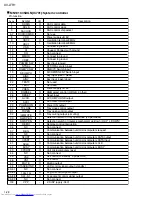
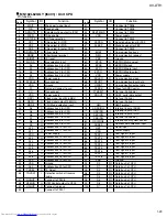
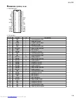
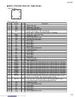
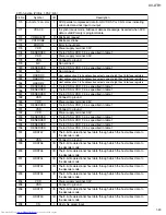
Pin No.
Symbol
RD
R/W
VDD
WAIT
RESET
VSS
VDD
INT
NC
NC
NC
NC
VDD
VSS
NC
NC
NC
NC
VSS
VDD
VDATA0
VDATA1
VDATA2
VDATA3
VDATA4
VDATA5
VDATA6
VDATA7
VSYNC
HSYNC
VSS
VDD
NC
NC
NC
VDD
I/O
Description
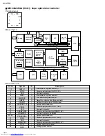
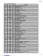
2.Pin function (1/5)
Read strobe input
Read/write strobe input
Power supply terminal 3.3V
Transfer not complete / data acknowledge.
Active LOW to indicate host initiated transfer is complete.
Active LOW : reset signal input
Connect to ground
Power supply terminal 3.3V
Host interrupt signal output
Non connect
Non connect
Non connect
Non connect
Power supply terminal 2.5V
Connect to ground
Non connect
Non connect
Non connect
Non connect
Connect to ground
Power supply 3.3V
Video data bus output. Byte serial CbYCrY data synchronous with VCLK.
Video data bus output. Byte serial CbYCrY data synchronous with VCLK.
Video data bus output. Byte serial CbYCrY data synchronous with VCLK.
Video data bus output. Byte serial CbYCrY data synchronous with VCLK.
Video data bus output. Byte serial CbYCrY data synchronous with VCLK.
Video data bus output. Byte serial CbYCrY data synchronous with VCLK.
Video data bus output. Byte serial CbYCrY data synchronous with VCLK.
Video data bus output. Byte serial CbYCrY data synchronous with VCLK.
Vertical sync. Bi-directional, the decoder output the top border of a new
field on the first HSYNC after the falling edge of VSYNC.
Horizontal sync. The decoder begins outputting pixel data for a new
horizontal line after the falling (active) edge of HSYNC.
Connect to ground
Power supply terminal 3.3V
Non connect
Non connect
Non connect
Power supply terminal 2.5V
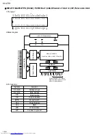
ZIVA-4.1-PA2(IC501):Back end - Digital decoder
1
52
156
105
208 157
53 104
~
~
~
~
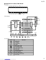
1.Terminal layout

