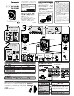
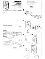
background image

2-3

XM-R700SL

I

H

A

B

C

D

E

F

G

1

2

3

4

5

6

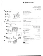
Standard schematic diagrams

MD servo & main amp section

ANALOG PB SIGNAL

DIGITAL PB SIGNAL

ANALOG REC SIGNAL

DIGITAL REC SGNAL

TP502

R807

C808

R820

R466

R402

R368

C457

IC351

C865

R351

L501

R527

C456

CN551

CN552

R501

C252

R352

C152

C202

R353

R503

C826

IC803

C817

S552

K221

J851

K121

K821

IC821

C205

TH501

K201

IC300

C223

K801

K852

C319

C318

K251

K151

C105

IC400

D400

L400

C317

C316

L404

L402

L403

L405

C406

C407

C408

C409

C404

C402

C123

CN701

K101

C315

R329

R328

K851

C505

R327

R325

R324

C314

K853

R354

C401

R355

S551

C313

R323

C807

R322

C320

C312

R356

C804

C801

IC504

CN300

R357

TP331

TP330

R358

R360

R318

R362

C106

R303

R363

R364

R365

R367

R366

R387

R517

R389

R300

C351

C362

R552

C352

R553

R388

IC341

R305

C102

R371

C341

C307

C306

R561

C343

R562

TP450

C864

C342

C508

R369

C354

C353

TP323

X351

R361

R359

C366

C575

R520

C574

C573

C357

C323

D301

R310

Q301

R531

R801

TP325

C308

TP324

TP328

C302

C356

R386

R385

C365

Q300

R376

R375

C358

TP505

R383

IC801

C802

R301

TP451

IC501

C803

S502

C403

C806

R382

R380

R378

R381

C552

R379

TP569

C360

C361

C863

TP335

TP309

TP308

C866

R104

R204

TP504

TP355

C206

C867

C868

R162

R307

R308

R515

R523

R525

C228

R514

D552

TP516

C128

R557

R554

R560

R559

C300

C303

R558

X500

C304

R326

IC502

R519

C507

IC802

R510

C305

C501

TP501

R502

C502

R551

CN401

R304

TP519

CN571

C571

C551

R572

R571

S501

C805

C503

C504

R806

R221

R121

D501

R556

IC821

IC822

IC823

IC824

R101

R201

C121

R262

C163

C263

TP510

R526

C463

R321

R555

IC301

R330

R331

C322

C321

C221

R400

R205

R105

C222

C812

Q821

D504

TP332

TP319

R822

C822

C821

R524

R455

R451

R450

R317

C455

C454

C506

R166

R266

C162

C262

C161

C301

IC851

IC803

Q804

C861

R521

R859

R861

R862

C862

R152

C122

R222

R122

R252

R223

R123

C261

R261

R161

C151

C251

R812

IC825

R829

J801

R821

R224

R124

C224

C124

C226

C126

R813

Q801

R811

C814

Q803

C813

K854

Q802

R863

C201

C101

R226

R227

R203

R103

R814

R815

C815

Q822

R827

R828

R817

R816

C810

C811

R125

IC450

J821

R127

R126

C225

C227

C125

C127

R823

R824

C824

C823

R825

C825

R202

R102

R826

R128

R228

R229

D821

R129

K802

K803

TP506

TP507

TP508

TP321

R311

R312

R313

Q342

R314

R341

TP537

C458

R528

R529

R530

R316

R315

R370

C450

R372

R306

R373

R374

R465

R302

R384

R377

C359

R505

R506

R507

R508

R509

R522

C572

D503

R251

R151

R504

C461

C460

R461

R460

R459

C459

R225

2.2k

1

100

1

1

2.2k

0.001

CXD2672GA

0.1

1k

NQL302N-100X

NI

0.0022

QGF0513F2-07X

QGF0513F1-06X

2.2K

1

1k

1

NI

1k

NI

330p

NI

330p

NSW0117-001X

QNS0098-002

NJM2115V-W

NI

NAD0021-103X

CXA2523AR

0.1

0.1

0.022

NI

MPC17A139MTB-X

F02J4L-X

NQL114K-471X

0.01

0.22

NQL365K-100X

NQL365K-100X

NQL365K-100X

NQL365K-100X

3.3/16

3.3/16

3.3/16

3.3/16

1

3.3/16

0.1

QGF0513F1-05X

0.0068

100

330

0.1

330

1K

330

1

1k

10/6.3

1k

QSW0678-001X

0.0047

330

0.1

330

0.1

1

1k

NI

0.1

IC-PST3424U-X

QGF0513F2-22X

1k

1k

1k

13k

1k

1

2.2K

1k

1k

1k

1k

1k

1

100K

1

22

10/6.3

10/6.3

2.2k

10/6.3

2.7k

1

TK11224BMC-X

330

NI

470

0.1

0.022

0.0068

68k

10/6.3

120k

1

0.1

1

100

7P

7P

NAX0439-001X

10k

10k

0.1

220p

220K

220p

220p

0.47

0.1

1SS355-X

18K

DTA144EE-X

100k

10

0.001

0.01

0.01

10k

10k

0.1

2SB1219/RS/-X

100k

10k

1

220

AK4562VN-W

3.3/4

0.22

HD6433048SV67X

0.1

NSW0121-001X

1

NI

150

1k

3.3k

1M

0.01

1k

0.47

0.015

0.1

330p

0

0

1

330p

330p

3.9k

2.2K

10K

1k

220K

100k

0.1

470K

1SS388-X

0.1

15k

3.9k

39k

27k

0.1

10/6.3

18k

NAX0248-001X

0.01

4.7K

AK93C55BH-W

330K

1

TK11225BMC-X

470k

0.001

10/6.3

27K

0.01

10k

QGF0513F2-16X

470k

QGF0513F1-07X

1

0.01

10k

10k

NSW0099-001X

0.1

0.1

0.1

470

4.7k

4.7k

1SS388-X

100k

NJM2115V-W

UMW1N-W

UMW2N-W

UMW1N-W

47k

47k

330P

3.9k

0.22

0.22

100K

10/6.3

56K

5.6k

SN74AHC1G08DC-X

2.2k

2.2k

0.022

0.022

330P

100K

NI

NI

1/16

10/6.3

2SC4617/R/-X

1SS388-X

47k

10/6.3

100k

1

22K

22K

91k

0.1

1

0.1

10k

10k

150/4

150/4

0.22

10/6.3

JCV8002-W

NI

NI

10/6.3

10K

100K

100K

100K

4.7/4

3.3k

1/16

1k

1k

3.3k

100k

100k

0.22

10

10

330p

330p

1k

RN1964-X

10K

QNZ0416-001X

100k

1k

1k

3.3/4

3.3/4

10/6.3

10/6.3

100

DTA114EE-X

10k

NI

NI

0.1

DTC144EE-X

4.7

100p

100p

150

33k

NI

NI

15k

NI

NI

NI

2SA2018-X

100k

4.7k

NI

NI

0.1

0.1

15k

CXA8095Q

NNS0004-001X

33k

150

NI

270P

NI

270P

10k

10k

10/6.3

0.1

4.7M

3.3/10

NI

NI

2.7k

1M

1M

1k

DAP222-X

1k

1K

1K

1K

DTA114YE-X

1K

220

0.047

1k

1k

1k

24K

13K

100

0.047

220

470K

220

470

NI

100K

100k

680k

470P

100k

100k

100k

100k

100k

330K

1

1SS388-X

20k

20k

100k

10/6.3

0.047

0.0068

47K

680k

1M

2.2

XRST2

FCS-

I

LDON

EFMO

HEADGND

BATT

RFOFF

RFVCTL

TX

XINT

RECP

DQSY

SQSY

XRST

SENS

SRDT

SFDR

XLAT

SCLK

DGND

SYSCNT

SWDT

SVCC

MNT3

MHON

D

DTRF

CS

MNT2

MNT1

MNT0

MHON

RFVCTL

DADT

FE

FCS-

DIN

ADDT

BYPS

A

TE

FCS+

XRST2

MGND

MM-

TRDR

B

1.8V

RMDT

TFDR

FS4

FFDR

F

VCCAUDIO

SRDR

FRDR

AGND

SRDR

SFDR

TRK-

C

FRDR

FFDR

TFDR

TRDR

J

MMDRVDN

SLDIN

VC

E

SLDOUT

TRK+

BATTGND

EFMO

FCS+

REMOFF

TRK+

BOTM

ABCD

FE

TRK-

RMVCC

AUX1

SE

MMDRVUP

CPUGND

5.0V

TE

TX

CHARGE

CKRF

SPRD

XLRF

BATTGND

BATTGND

OPEN

SPFD

ADFG

SSTOP

MREF

SPFG

MPROT

MHUP

VCNTDA

FS4

MHDN

MMDRVUP

BATTGND

BATTGND

MMDRVDN

2.7V

MM+

LDON

RECP

RFOFF

INB

2.0V

PS

MM+

SLDOUT

PD

BOTM

RFGND

SLDIN

MECHAGND

ADDT

DADT

XBCK

FS256

LRCK

CDATA

COM

U

V

W

INA

VG

SCL

DI

XRST

XLAT

SWDT

SRDT

PEAK

SCLK

ABCD

AUX1

ADFG

APCREF

VREF

SE

APC

PSW

SPFG

PS

PSW

DTRF

CKRF

XLRF

PS

XBCK

CDATA

SPRD

SSTOP

BEEP

PDN

BATTERY

CLAT

LRCK

XBCK

FS256

PDN

W

BYPS

SPFD

RPLY

LCDDATA

V

KEYON

U

COM

LCDCLK

OPEN

PEAK

MUTE

SQSY

BATTSTATUS

LCDLAT

LCDLAT

DQSY

LCDCLK

BEEP

MREF

MPROT

MHUP

MHDN

MUTE

MICIN

OPTIN

EXTBATT

MNT2

MNT1

ACXDC

CCLK

LCDDATA

DO

ADPWR

UNREG

MICIN

AC/DC

MM-

CCLK

CLAT

FFCLR

MWUP

WAKEUP

RMDT

XINT

MNT0

MNT3

SENS

ADPWR

OPTIN

DIN

MICIN

MD servo & main amp section

Summary of Contents for XM-R700SL

Page 1: ...LTD XM R700SL XM R700SL Area Suffix US Singapore Contents Safety Precautions Important for laser products Attention when MD pick up is exchanged Disassembly method Adjustment method Maintenance of laser pickup Replacement of laser pickup Description of major ICs 1 2 1 3 1 4 1 5 1 15 1 17 1 17 1 18 37 ...

Page 2: ...urrnet check Electrical shock hazard testing After re assembling the product always perform an isolation check on the exposed metal parts of the product antenna terminals knobs metal cabinet screw heads headphone jack control shafts etc to be sure the product is safe to operate without danger of electrical shock Do not use a line isolation transformer during this check Plug the AC line cord direct...

Page 3: ...g laserstrålning är denna del är öppnad och spårren är urkopplad Betrakta ej strålen VARO Avattaessa ja suojalukitus ohitettaessa olet alttiina näkymättömälle lasersäteilylle Älä katso säteeseen ADVARSEL Usynlig laserstråling ved åbning når sikkerhedsafbrydere er ude af funktion Undgå udsættelse for stråling ADVARSEL Usynlig laserstråling ved åpning når sikkerhetsbryteren er avslott unngå utsettel...

Page 4: ...st the electrified static electricity to the human body 3 Handling the optical pick up 1 Please return according to a correct procedure based on short processing after exchanging parts 2 Do not use a tester to check the condition of the laser diode in the optical pick up The tester s internal power source can easily destroy the laser diode 4 Attention when unit is disassembled Please refer to Disa...

Page 5: ...ly and the bottom cover See Fig 1 to 6 Disconnect the flexible wires from connector CN522 and CN571 on the main board 3 Peel off the adhesive tapes attaching the flexible wires Whenreconnecting the flexible wires to the connectors fix them with adhesive tapes SeeFig 2 ATTENTION When reattaching the bottom cover fit the hole knobs b to the hold switches on the main board correctly See Fig 1 and 2 A...

Page 6: ...ng the main board See Fig 7 to 10 When pulling out the flexible wires get it through the opening of themain board and the cabinet ATTENTION Before disconnecting the flexible wire extending from the pickup makesure to solder the short circuit round to prevent damage to the pickup ATTENTION Peel off the adhesive tapes attaching the flexible wires Whenreconnecting the flexible wires to the connectors...

Page 7: ...e screw F attaching the main board and the cabinet assembly Remove the main body in the direction of the arrow while releasing the part d thenpart e of the cabinet assembly from the flame assembly 2 3 4 Removing the MD mechanism assembly See Fig 11 When reassembling connect the flexible wire extending from the pickupto the connector on the main board and unsolder the short circuit round ATTENTION ...

Page 8: ...move the MD door assembly and the bottom cover Remove the two screws I and the one screw J attaching the door plate on the inside of the MDdoor assembly Peel off the adhesive tape attaching the flexible wire Pull out the door plate assembly in the direction of the arrow from the part h on the MD doorassembly Remove the LCD assembly and the 5 key sheet from the door plate assembly They are attached...

Page 9: ... in the direction of the arrow Lift the right edge of the head protector See Fig 4 Pull the left tab of the head protector from the slit See Fig 5 Remove the two B screws attaching the magnetic head assembly on the underside of the chassis assembly Pull out the magnetic head assembly in the direction of the arrow while paying attention to the magnetic head Removal of the MD mechanism Fig 3 Fig 1 F...

Page 10: ... Remove the screw C of the chassis assembly part c and lift the edge of the holder assembly in the direction of the arrow d See Fig 3 Move the part e of the holder assembly in the direction of the arrow to release the U shaped notch from the shaft Pull the part f of the holder assembly in the direction of the arrow to release it from the shaft CAUTION When reassembling the magnetic head assembly r...

Page 11: ...D screws fixing the main shaft of the pickup unit on the underside of the chassis assembly Remove the pickup unit by pulling out the part g in the direction of the arrow Remove the screw E attaching the lead spring on the pickup unit Remove the main shaft from the pickup unit Fig 7 Fig 8 D Pickup unit Main shaft Part g Main shaft Pickup unit E Lead spring ...

Page 12: ...exible harness assembly and the protect reflect switch assembly respectively 4 Pull out the part k and l in the direction of the arrows respectively and remove the flexible harness assembly and the protective reflective switch assembly Fig 9 Fig 10 Fig 11 Flexible harness Feed motor Double sided tape Peel off Feed motor Peel off Part i unsoldering Part h unsoldering Part j unsoldering F F F Flexib...

Page 13: ...he lift motor with the lift motor bracket by pulling out the part k Removing the Spindle motor See Fig 14 1 Prior to performing the following procedure remove the flexible harness assembly Remove the three H screws attaching the spindle motor on the underside of the chassis assembly Fig 8 Part k Lift motor bracket G G Part j unsoldering Lift motor Pull out Lift motor bracket Flexible harness assem...

Page 14: ...the chassis assembly Unsolder the part i of the flexible harness connected to the feed motor Remove the two I screws attaching the feed motor base then the feed motor base and the feed motor When connecting the flexible harness to the feed motor use the double sided tape to stick them fast See Fig 17 Flexible harness Feed motor Double sided tape Flexible harness Feed motor Double sided tape Peel o...

Page 15: ...sert the laser power meter sensor Adjust more than 875 W and more cross this Select Press PLAY key Adjustment DISC Pre mastered PRE DISC TGYS 1 Recordable MO DISC AU 1 or full recorded normality set 80min tracking off set adjust SONY 80min DISC Continue next page servo initialize Play laser Rec laser LCD full on then indicate TEST MODE Select the item by F SKIP B SKIP key Adjust the voltage to les...

Page 16: ...C AU 1 Press PLAY key Start the adjustment auto adjustment Complete the adjustment Press STOP key then eject DISC Select R_TOF AUTO Insert the adjustment DISC SONY 80min DISC Press PLAY key Start adjustment auto adjustment Complete the adjustment Press STOP key then eject DISC Power off by release the AC adapter LCD indication LCD indication From the previous page Adjust the laser power by F SKIP ...

Page 17: ...life of the laser diode has expired the following symptoms will appear 1 The level of RF output EFM output ampli tude of eye pattern will below Is the level of RFOUT under 0 35Vp p Replace it NO YES O K 3 Semi fixed resistor on the APC PC board The semi fixed resistor on the APC printed circuit board which is attached to the pickup is used to adjust the laser power Since this adjustment should be ...

Page 18: ...put for main beam servo signal B current input for main beam servo signal C current input for main beam servo signal D current input for main beam servo signal E current input for side beam servo signal F current input for side beam servo signal Reflection light quantity monitor signal input Laser APC output Reference voltage input for the laser power intensity setting Connect to GND Connects the ...

Page 19: ...tput Reflection light quantity signal output for the main beam servo detector RF ABCD bottom hold signal output Peak hold signal output for the RF ABCD signals RF equalizer output Connects the RFAGC capacitor RFAGC input User comparator output User comparator non inverted input Connects the capacitor for ADIP amplifier feedback circuit User operational amplifier output User operational amplifier i...

Page 20: ...OMF CPOUT CPC3 CP3 CPC2 CP2 CPC1 CP1 VCO RMAX RMIN VCOIN VCC MCLOCK CLKSEL S S BRAKE VCONT VCREF GND PGND FG2 FG SLOPE F R Controllor Timing controllor Phase Comparator 1 8 PWM VCO Full Wave Rectifilter Sensoeless Logic Charge Pump Voltage Driver Sample and Hard 1 Pin layout 2 Block diagram 1 12 36 25 37 48 24 13 ...

Page 21: ... maximum oscillation frequency of VCO The terminal to set minimum oscillation frequency of VCO The terminal to control oscillation frequency of VCO The terminal to select inside and outside clock The terminal to oscillation sawtooth for PWM signal The terminal to oscillation sawtooth for soft switching signal The terminal to monitor CLOCK signal The GND for the part except the power section The te...

Page 22: ... RFI AVD1 MVCI PD0 A11 XOE FRDR FFDR VDC4 VSC4 SRDR FS4 SPFD SPRD SFDR TEST2 TEST1 FGIN TST2 EFM0 TEST3 VSI03 TST3 VDI03 SPCU SPDW SPDV TST4 SPCW SPCV VSC5 SLDW SLDV SLCV SLCU VDC5 BYPS TST5 SLCW DVDD1 D3 VSC3 VDC3 D0 D2 D1 XCAS IXWE A09 XRAS IXOE A07 A10 A08 DVI01 A00 VSI01 A05 A01 A06 A03 A04 A02 F256 XBCK VSC2 VDC2 DADT LRCK VDI00 TST8 ADDT MNT1 MNT0 VDC0 SENS XRST RPWR VDI OSC DVDD0 DA VDDL DA...

Page 23: ... tal osc circuit input OSC sel VDD 2 5V X tal osc circuit output Internal 16bit DRAM GND Internal 16bit DRAM GND OSC sel GND Internal DAC Lch output Internal DAC VDD Lch 2 5V Internal DAC GND Internal DAC GND VREF Lch Internal DAC VDD Rch 2 5V Internal DAC GND Rch Internal DAC Rch output Internal DAC VREF Rch Internal logic GND X tal frequency select L 45 1584MHz H 22 5792MHz Test terminal Connect...

Page 24: ...a input output Internal 16Mbit DRAM VDD Open Open External DRAM output chip enable output Open Open Open Internal 16Mbit DRAM GND External DRAM write enable output Analog PLL phase compare output Playback EFM comparator slice level input Playback EFM binarization signal output Clock input from external VCO Analog GND Playback EFM comparator bias current input Analog power supply 2 5V Filter input ...

Page 25: ...ervo drive PWM output Internal logic VDD 1 8V Internal logic GND Sled servo drive PWM output 176 4kHz clock output X tal system Spindle servo drive output Spindle servo drive output Sled servo drive PWM output Test terminal Connect to GND Test terminal Connect to GND Spindle CAV servo FG input Test terminal Open EFM output at recording Test terminal Connect to GND 2 5V I O Vss Test terminal Open 2...

Page 26: ...O3 PGND RO3 VD3 VD4 RO4 PGND FO4 VD4 RI3 FI3 FI4 RI4 AGND CLK PS OE VD1 FO1 PGND RO1 VD1 VD2 RO2 PGND FO2 VD2 RI1 FI1 FI2 RI2 1 Pin layout 2 Pin function Clock detector Driver CLK PS OSC circuit X H H L Auto Synchronization Stop X PS OE INPUT OUTPUT 1 4 PS H H H H H L OE L L L L H X FI L L H H X X RI L H L H X X FO L L H L L Z RO L H L L L Z X Don t care Z High impedance ...

Page 27: ... VD4 FO4 RO4 PGND RGND VG VG VG Vc Vc Vc Vc CLK PS FI1 RI1 GND FI2 RI2 FI3 RI3 FI4 RI4 OE CLOCK CLK Detector DC DC Converter Control Control Control Control Pre driver Pre driver Pre driver Pre driver 1 5 9 36 34 14 10 6 8 7 12 30 13 11 32 28 31 29 23 27 24 26 25 21 18 17 33 15 16 4 3 2 35 22 19 20 3 Block diagram ...

Page 28: ...in 0 45 x VA Analog Ground Pin Analog Power Supply Pin 2 5V Analog voltage Reference Input Pin Used as a voltage reference of ADC DAC VREF is connected externally to filterd VA Digital power supply Pin 2 5V Digital Ground Pin Digital Interface Power Suooly Pin Audio Serial Data Output Pin Audio Serial Data Intput Pin Audio Serial Data Clock Pin Test Mode Pin Fixed to L Master Clock Input Pin Input...

Page 29: ... OUT V Power amplifier output GND in power amplifier output steps Power amplifier output Symbol FUNCTION CC2 CC2 A B 2 2 1 ref ref CC1 CC B A B BEEP OUTA 3 Pin function Pin no B in power amplifier output steps Smoothness of level detection of boost BST amplifier input signal level variable control by input lever to boost AGC input terminal Output terminal of BST amplifier2 Terminal NF of BST ampli...

Page 30: ... Pin function DO EEPROM 2048bit 128 X 16 16 16 R W AMPS AND AUTO ERASE DECODER DATA REGISTER ADD BUFFER INSTRUCTION DECODE CONTROL AND CLOCK GENERATION INSTRUCTION REGISTER DI CS SK PE VREF VPP SW VPP GENERATOR Fnction 1 2 3 4 5 6 7 8 9 10 20 19 18 17 16 15 14 13 12 11 G1 A1 A2 A3 A4 A5 A6 A7 A8 GND Vcc G2 Y1 Y2 Y3 Y4 Y5 Y6 Y7 Y8 Input Output G1 H X L L G2 X H L L An X X H L Yn Z Z H L SN74AHCT540...

Page 31: ...cable connect detection Ground Non use Power save control output of A D section Driver power supply control signal output Data output for LCD clock output for LCD Latch output for LCD Pin No Symbol I O Pin function 51 52 53 54 55 56 57 58 59 60 61 62 63 64 65 66 67 68 69 70 71 72 73 74 75 76 77 78 79 80 81 82 83 84 85 86 87 88 89 90 91 92 93 94 95 96 97 98 99 100 DATA CLK LAT JOG JOG GND SYSCNY CH...

Page 32: ...24U X IC504 Reset 1 Pin layout 2 Block diagram 3 Pin function 1 2 VOUT VDD 4 3 VSS NC 1 VOUT 2 3 VDD VSS Vref 1 2 3 4 Reset Signal Output PIN VDD PIN Voltage Detect PIN Non connect VSS PIN Vout VDD NC VSS No Pin Name Function ...

Page 33: ...l pin Boot capacitor connection pin Boot capacitor connection pin Power supply pin Totem pole type output pin Output current setting pin Ground pin Soft start setting capacitor connection pin Short detection setting capacitor connection pin Powersupplycontrolpin WhenthispinisHigh ICisinactivestate WhenthispinisLow ICisstandbystate Reference voltage output pin I I O I O I O I O Function FB IN IN DT...

Page 34: ...XM R700SL 1 34 NJM2115V W IC821 Regulator 1 Pin layout 2 Block diagram A B 1 A OUTPUT 2 A INPUT 3 A INPUT 4 V 8 V 7 B OUTPUT 6 B INPUT 5 B INPUT INPUT INPUT V V OUTPUT ...

Page 35: ...N OFF VOUT CONT Protect circuit PFM Control circuit VREF 1 2 3 4 5 Power off terminal Voltage output terminal N C Terminal Ext indnctor Connection terminal ON OFF VOUT VSS CONT No Pin Name Function TK1125BMC X IC802 Regulator 1 Pin layout 2 Block diagram GND VIN CONT THERMAL SENSOR BANDGAP REFERENC Cnp VOUT ...

Page 36: ...XM R700SL 1 36 TK1124BMC X IC341 Regulator 1 Pin layout 2 Block diagram GND VIN CONT THERMAL SENSOR BANDGAP REFERENC Cnp VOUT ...

Page 37: ...nction 1 2 3 4 5 EXT VDD GND CE FB No Pin Name Function 5 1 2 3 4 Buffer Driver Phase Compensation PWM Conparator Ramp Wave Generator OSC PWM PFM Contoroler Vref with Soft Start CE Error Amp VDD EXT GND FB CE EXT transistor connect Power supply GND Chip enable Output voltage setting ...

Page 38: ...nted in Japan 200101 O VICTOR COMPANY OF JAPAN LIMITED AUDIO COMMUNICATION BUSINESS DIVISION PERSONAL MOBILE NETWORK BUSINESS UNIT 10 1 1chome Ohwatari machi Maebashi city 371 8543 Japan No 20991 XM R700SL ...

Page 39: ...CN300 CN701 MAGNETIC HEAD CN602 CN601 IC601 BUFFER MHON EFM JOG JOG KEY1 KEY2 LCDDATA LCDCLK LCDLAT RESET SCL DI DO RMDT OUTA OUTB MHON PS MM MM VG W V U COM MHDN MHUP SSTOP MREF MPROT PS SLDIN SLDOUT MMDRVUP MMDRVDN SPFD SPRD SPFG FCS FCS A B C D E F I J PD PEAK BOTOM ABCD FE AUX1 ADFG SE TE RF APCREF DIN CCLK CLAT PDN PSW MUTE BEEP OPTIN LOUT1 ROUT1 LIN2 RIN2 LIN1 RIN1 ADDT DADT LRCK XBCK FS256 ...

Page 40: ...2 2 XM R700SL M E M O ...

Page 41: ...1 3 3 16 0 1 QGF0513F1 05X 0 0068 100 330 0 1 330 1K 330 1 1k 10 6 3 1k QSW0678 001X 0 0047 330 0 1 330 0 1 1 1k NI 0 1 IC PST3424U X QGF0513F2 22X 1k 1k 1k 13k 1k 1 2 2K 1k 1k 1k 1k 1k 1 100K 1 22 10 6 3 10 6 3 2 2k 10 6 3 2 7k 1 TK11224BMC X 330 NI 470 0 1 0 022 0 0068 68k 10 6 3 120k 1 0 1 1 100 7P 7P NAX0439 001X 10k 10k 0 1 220p 220K 220p 220p 0 47 0 1 1SS355 X 18K DTA144EE X 100k 10 0 001 0 ...

Page 42: ... SIGNAL IC601 D602 D601 R605 R606 R601 R602 R603 R604 R608 R607 C604 C603 C602 C601 Q601 Q603 Q602 Q604 CN602 CN601 Q605 SN74AHCT540PW X FS05J10 X FS05J10 X 220k 22k 220k 220k 220k 220k 2 2 100p 100 0 1 10 10 0 1 2SK2315 W 2SK2315 W 2SK2315 W 2SK2315 W QGF0513F1 05X QGF0513F1 05X DTC144EE X ...

Page 43: ... 330X 22 4 8 2k 10K NI NQL114M 1R0X 22 4 1K F1J2E X MB3817PFV X 2 2 0 1 0 01 1000P 5 6K 270K 18K 0 033 SSM3J01F X NI 0 001 QNA0023 001 F1J2E X 2SA1774 R X 1 5 220 4 7 1SS355 X CRS01 W NQL32CM 470X 22 4 200K 180k XC6366B102M X S 8321AAMPDNA W 1 0 NQL114K 331X MA729 X 1 5 1SS388 X NSW0121 001X SI2305DS X NI 1 5 1 5 10 10 220P 330K 220K 1 0 470K 10K 10K 47k 2SA1774 R X 0 01 TK11118SC W 1 220K 2SC4617...

Page 44: ...C162 K151 R166 K851 C866 K251 R266 J851 R863 C867 K852 K802 Q801 R811 R104 C865 Q802 K853 C868 K803 K201 K101 C101 R101 K801 R102 C102 C864 C802 C817 C201 C202 R202 R201 C222 R222 R223 R203 R103 IC803 C121 C122 R123 R123 C223 IC823 R124 C123 R125 C124 C224 R562 R224 C125 R225 C225 C814 S552 C815 R815 R814 IC821 C804 R801 C862 C801 C106 C206 C803 C805 C807 C806 R372 R371 R806 IC801 R823 R824 C824 R...

Page 45: ... assemblies are not available as service parts Contents Exploded view of general assembly and parts list MD mechanism assembly and parts list Electrical parts list Packing materials and accessories parts list XM R700SL 3 3 3 6 3 8 3 12 Area suffix US Singapore ...

Page 46: ...XM R700SL 3 2 M E M O ...

Page 47: ...nd parts list Block No M M M 1 Magnetic head board Main board 32 43 30 45 47 31 43 36 33 35 41 44 40 39 38 42 56 53 56 56 49 57 57 52 51 50 37 55 55 25 29 25 26 28 15 14 16 13 17 11 12 27 24 23 6 4 7 8 5 22 22 18 19 48 48 46 9 10 20 20 3 21 2 34 1 54 ...

Page 48: ... MECHA 21 LV30225 032A CUSHION 1 22 LV40406 001A SPECIAL SCREW 2 FOR MECHA 23 LV41237 001A INSULATOR 1 FOR JACK 24 LV41237 002A INSULATOR 1 FOR JACK 25 VKZ4616 008 SCREW 2 FOR PCB 26 QYSPSPU1425N SCREW 1 27 LV30225 033A SPACER 1 FOR PCB 28 F00411 02 LUG TERMINAL 1 29 LV30225 036A SPACER 1 FOR PCB 30 LV32648 002A MD DOOR ASSY 1 31 LV31186 002A SET BUTTON 1 32 LV31190 003A ESCUTCHEON 1 33 LV31183 00...

Page 49: ...49 LV20433 006A BOTTOM COVER A 1 FOR JES PRODUCT 50 LV41043 001A INSULATOR 1 FOR BOTTOM COVE 51 LV31191 001A H P JACK COVER 1 52 LV31192 001A DC JACK COVER 1 53 LV31187 001A SLIDE KNOB 2 54 QUQ605 0506AA FFC WIRE 1 55 LV41237 003A INSULATOR 3 56 VKZ4616 008 SCREW 4 FOR BOTTOM COVER 57 LV41215 003A MINI SCREW 2 ...

Page 50: ... 28 31 29 1 30 19 17 15 27 14 18 26 26 11 16 25 12 21 20 5 25 24 13 4 27 2 10 3 10 3 22 23 8 7 6 9 CFD4007HYZ FG 87HS MOBIL 1 MD mechanism assembly and parts list Block No M M M 2 Grease FLM SRM2 14 0 45 0 1mm 15 11 ...

Page 51: ...ASSY 1 12 LV40921 002A L WHEEL GEAR 1 13 WDM082520 SLIT WASHER 1 14 LV40920 001A L WORM GEAR 1 15 QAR0096 001 MOTOR 1 16 LV40931 001A SPECIAL SCREW 2 M1X1 2 17 LV41228 001A TORSION SPRING 1 18 LV40501 001A SPECIAL SCREW 2 M1 4X1 6 19 LV31053 001A LIFT SLIDER 1 20 LV40922 001A LIFT GEAR 1 21 WDM082520 SLIT WASHER 1 22 QAH0031 001 MD HEAD 1 23 LV41020 001A SPECIAL SCREW 2 M1 7X2 0 24 QAR0053 001 SPI...

Page 52: ...CK 474X C CAPACITOR C 358 NCB21AK 105X C CAPACITOR C 359 NCS31HJ 471X C CAPACITOR C 360 NCB21CK 474X C CAPACITOR C 361 NCB31HK 153X C CAPACITOR C 362 NBE20JM 106X E CAPACITOR C 365 NCB31CK 104X C CAPACITOR C 366 NCB31CK 104X C CAPACITOR C 401 NBE90JM 106X E CAPACITOR C 402 NBE21CM 335X E CAPACITOR C 403 NCB21AK 105X C CAPACITOR C 404 NCB21AK 105X C CAPACITOR C 406 NBE21CM 335X E CAPACITOR C 407 NB...

Page 53: ... IC IC502 AK93C55BH W IC IC504 IC PST3424U X IC IC801 AK4562VN W IC IC802 TK11225BMC X IC IC821 NJM2115V W IC IC822 UMW1N W TRANSISTOR IC823 UMW2N W TRANSISTOR IC824 UMW1N W TRANSISTOR IC825 RN1964 X TRANSISTOR IC851 JCV8002 W IC IC911 MB3817PFV X IC IC921 XC6366B102M X IC IC931 S 8321AAMPDNA W IC IC941 TK11118SC W IC IC951 TC7W00FU X IC J 801 QNZ0416 001X LINE OPT JACK J 821 NNS0004 001X 3 5 JACK...

Page 54: ...3J 102X MG RESISTOR R 352 NRSA63J 102X MG RESISTOR R 353 NRSA63J 102X MG RESISTOR R 354 NRSA63J 102X MG RESISTOR R 355 NRSA63J 102X MG RESISTOR R 356 NRSA63J 102X MG RESISTOR R 357 NRSA63J 102X MG RESISTOR R 358 NRSA63J 102X MG RESISTOR R 359 NRSA63J 103X MG RESISTOR R 360 NRSA63J 102X MG RESISTOR R 361 NRSA63J 103X MG RESISTOR R 362 NRSA6AJ 102W MG RESISTOR R 363 NRSA63J 102X MG RESISTOR R 364 NR...

Page 55: ...STER R 922 NRVA63D 184X MG RESISTOR R 923 NRSA63J 2R2X MG RESISTOR R 941 NRV142F 1R5X MG RESISTOR R 942 NRV142F 1R5X MG RESISTOR R 943 NRV142F 1R5X MG RESISTOR R 944 NRV142F 1R5X MG RESISTOR R 951 NRSA63J 560X MG RESISTOR R 952 NRSA63J 473X MG RESISTOR R 953 NRSA63J 474X MG RESISTOR R 954 NRSA63J 474X MG RESISTOR R 955 NRSA63J 474X MG RESISTOR R 956 NRSA63J 274X MG RESISTOR R 957 NRSA63J 104X MG R...

Page 56: ...XM R700SL 3 12 P3 P2 P1 A8 A9 A10 A2 A4 A5 A6 A1 A7 A3 P4 Packing materials and accessories parts list Block No M M M 3 Block No M M M 4 ...

Page 57: ...N 1 Item Parts number Parts name Area A Parts list Accessories Q ty Description Block No M4MM A 1 LVT0621 004A INSTRUCTIONS A 1 A 2 QAB0021 002 LI ION BATTERY A 1 BN R3610 ENG SPA CHI A 3 QAL0181 001 AC ADAPTOR A 1 A 4 QAN0021 002 HEAD PHONE 1 A 5 QAL0252 004 REMOCON 1 A 6 LV31256 002A BATT CASE ASSY 1 A 7 LV32289 001A SOFT CASE 1 A 8 QMP39F0 183E POWER CORD A 1 A 9 QAM0060 001 SIEMENS PLUG 1 A 10...

Reviews: