TV-20F242
TV-20F242
No.51768
No.51768
&
2-13
2-14
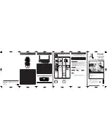
CIRCUIT DIAGRAM
[SYSCON PCB CHROMA/IF SCHEMATIC DIAGRAM]
A
B
C
D
E
F
G
H
A
B
C
D
E
F
G
H
2
1
3
4
5
6
7
8
2
1
3
4
5
6
7
8
CF602
MKT47.3MC110P
CP602_1
8283_0712_00_000
1
2
3
4
5
6
7
C665_1
10
16V
KANP
TU601
NJH3022U268
1
10
11
12
13
14
15
2
3
4
5
6
7
8
9
OUT
OUT
G
IN
IN
CF601
SAF45MFY220ZR
SAW FILTER
1
2
3
4
5
CF603
EFCT4R5YS5A
CF604
EFCT4R5MW5
IC601
M61203CFP
CHROMA
1
10
11
12
13
14
15
16
17
18
19
2
20
21
22
23
24
25
26
27
28
29
3
30
31
32
33
34
35
36
37
38
39
4
40
41
42
43
44
45
46
47
48
49
5
50
51
52
53
54
55
56
57
58
59
6
60
61
62
63
64
7
8
9
L617
HF57T18.5*10*10
CD601_1 CH2D068A
1
10
11
12
13
2
3
4
5
6
7
8
9
VR6001_1
4.7K
SEP.
CD4205
CH01812A
1
THE DC VOLTAGE AT EACH PART WAS MEASURED
WITH THE DIGITAL TESTER WHEN THE COLOR BROADCAST
WAS RECEIVED IN GOOD CONDITION AND PICTURE IS NORMAL.
NOTE:
D601 1SS133
D607
1SS133
D605
11ES1N
D617
1SS133
D616
1SS133
D618
1SS133
CD850
CH25086A
1
2
3
4
5
DANS LA NOMENCLATURE DES PIECES
N’UTILISER QUE CELLS DECRITES
DANGEREUSES AN POINT DE VUE SECURITE
ETANT
LES PIECES REPAREES PAR UN
ATTENTION:
DESCRIBED IN PARTS LIST ONLY
CRITICAL FOR SAFETY,USE ONES
ARE
SINCE THESE PARTS MARKED BY
CAUTION:
IS NON POLAR ONE.
THE ALUMI ELECTROLYTIC CAPACITOR MARKED NP
THE RESISTOR MARKED F IS FUSE RESISTOR.
NOTE:
DEFLECTION SIGNAL
G.SIGNAL
R.SIGNAL
B.SIGNAL
L613
2.2uH
L605
2.7uH
L620
47uH
L614
6.8uH
L607
10uH
L602
2.7uH
L618
33uH
Q607
2SC2412K
BUFFER
Q612
2SC3000
PRI.AMP
Q601
2SA1037AK
BUFFER
X602
100CT3R505
3.579545MHz
C687
150P
B
C675
0.1 B
C674_1
0.1 B
C634
0.01 B
C639
0.01
B
C637
0.01
B
C661
0.01 B
C648
0.1 M
C629
22
CH
C627
1 B
C618
5P CH
C671
220P CH
C663
390P CH
C623_1
68P CH
C613
0.1 B
C622
0.22 B
C616
0.01
B
C636
0.01
B
C640
0.1
B
C625
1 F
C626
0.1 B
C621
0.01 B
C664
1 MMTS
C615
0.001 CH
C658
0.22 B
C644
0.022 B
C650
0.015
B
C630
0.022 B
C614
0.01
B
C602_1
0.1 F
C653
0.01
B
C660
0.1
B
C656
1 B
C654
18P
C
H
C676
82P CH
C647
0.01
B
C609
0.1
B
C607
0.1
B
C669
0.1 B
R671
1K
R601
2.2K
R674
47
1/2W
R605
22K
R603
220
1
/4W
R602
220
1
/4W
R632
33
R621
1K
R656
2.2K
R626
10K
R624
2K
R627
10K
1/4W
R657
1K
R684
2.2K
1/4W
R646
15K
R638
6.8K
R611
10K
R608
10K
R618
10M
R607
220 1/2W
R609
330
R643
47K
R642
6.8K
R670
100
R673
150K
R625
10K
R614
180K
R633
8.2K
R616
220
R622
390
R620
12K
R647
2.2K
R648
2.2K
R652
4.7K
R610
100 1/4W
R672
470
R629
2.2K
R680
5.6K
R665
1K
R6001
1K
(C6008)
R677
3.3M
R634
100
R636
100
R635
100
R630
100
R655
100
R641 27K
R649 2.2K
R683
2.2K
R685
2.2K
1/4W
R681
1K
R628
6.8K
R631
6.8K
R659
2.2K
R658
2.2K
R660
2.2K
C610
2.2
50V
K
A
C635
47
16V
KA
C641
220
25V
YK
C624
47
16V
KA
C668_1
22
50V
KA
C649
1
50V
K
A
C645
1
50V
K
A
C612
220
6.3V
YK
C632
2.2
50V
KA
C620
47
6.3V
KA
C601
1
50V KA
C655
47
16V
KA
C659
47
16V
KA
W813
W825
W809
W876
W949
W804
W956
W937
(R6015)
W955
W938
(R6036)
L615
100uH
0607
L616
100uH
0607
L610
100uH
0607
L608
100uH
L603
100uH
D615
MTZJ6.8B
D602
MTZJ8.2C
D614
MTZJ6.8B
D609
MTZJ6.8B
D608
MTZJ6.8B
D613
MTZJ6.8B
D612
MTZJ6.8B
CP604
IMSA-9130B-06
1
2
3
4
5
6
OF PRINTING AND SUBJECT TO CHANGE WITHOUT NOTICE
NOTE: THIS SCHEMATIC DIAGRAM IS THE LATEST AT THE TIME
S811X
S811Y
S817Y
S824Y
S817X_1
S824X_1
AUDIO SIGNAL(REC)
TUNER VIDEO SIGNAL
IIC_OFF
DEGAUSS_H
8.7VREF
POWER_FAIL[DC]
5.7VREF[AT]
5.7VREF[PCON]
P.CON+5V
VD
OSD_R
OSD_G
OSD_B
OSD_BLK
SDA
MONITOR_V
SCL
AFT_M
VCR_POWER_H
HD
TU1_VIDEO
TV_POWER_H
TU1_AUDIO_A
X_RAY_TEST
TU1_VIDEO
MONITOR_V
SOUND+B
SOUND_GND
B.OUT
AGC_M
ACL
TU1_AUDIO_A
VD
OSD_BLK
SOUND+B
SOUND_GND
H_OUT
V_OUT
ACL
H_PLUSE
TV_POWER_H
POWER_FAIL[DC]
AFT_M
X_RAY_TEST
VCR_POWER_H
DEGAUSS_H
AGC_M
V_OUT
HD
OSD_B
OSD_G
OSD_R
AT+30V
GND
P.CON+5V[TU1]
P.CON+5V[CHROMA]
P.CON+8V
8.7VREF
5.7VREF[PCON]
5.7VREF[AT]
AT+13V
P.CON+5V
VCR_POWER_H
G.OUT
H_PLUSE
H_OUT
R.OUT
G.OUT
B.OUT
SCL
SDA
R.OUT
B.OUT
FROM/TO DEFLECTION
(CY901)
FROM/TO POWER
FROM/TO MICON
(CP805)
29
2.5
12.4
3.1
GND
FROM/TO CHASSIS
PCB010
VMX188
CUT OFF
(CP820)
MONITOR V.OUT
Y IN
C IN
GND
FSC
P.CON+5V
FROM/TO HIFI
FROM/TO Y/C/A/H.AMP
NC
NC
NC
TEST POINT
INTELLGENT MONI
FBP IN
SCL
RF AGC OUT
AFT OUT
VIF GND
VIF VIDEO OUT
QIF IN
VIF APC FILTER
VREG Vcc
VIF VCO F/B
AUDIO BYPASS
EXT AUDIO IN
FM DIRECT OUT
Hi Vcc
R OUT
AFC FILTER
DEF
H OUT
SDA
H VCO F/B
POWER ON CONT
STRAT UP Vcc
B IN
V RAMP FEEDBACK
V RAMP CAP
VIDEO CHROMA Vcc
fsc OUT
V PULSE OUT
CHROMA APC FILTER
TV/Y IN
5v REG
Y SW OUT
VIDEO/CHROMA GND
FAST BLK
SPOT KILLER
G OUT
RF AGC FILTER
INTELLIGENT MONI
MCU RESET
VIF Vcc
5.7V REG OUT(FOR CPU)
47 LIMITER IN
48 IF AGC
49 QIF OUT
50 AUDIO OUT
46 SW REG CONT
34 EXT C in
33 8.7V REG OUT
32 X’TAL
31 ACL/ABCL
64 VIF IN
1 VIF IN
17 V OUT
16 B OUT
H.PLUSE OUT
B.OUT
R.OUT
G.OUT
GND
GND
H.OUT
SOUND GND
SOUND+B
TV POWER H
H.PLUSE
ACL
V.OUT
V.FEEDBACK
POWER FAIL
X-RAY TEST
VCR POWER H
DEGAUSS H
2.7
0
2.0
7.2
0.8
2.0
2.0
8.2
8.2
8.2
4.0
5.5
5.6
0
0
3.2
3.2
2.0
8.8
3.3
3.0
0
4.7
0
0.1
7.3
4.9
4.9
4.8
2.0
0
8.5
8.5
3.8
1.5
5.0
5.0
2.6
3.6
0.8
2.5
0
0
3.6
3.4
3.9
4.8
2.5
2.5
2.4
2.3
2.4
2.3
3.0
2.0
3.2
9.0
3.0
2.2
0
0
2.4
2.9
2.3
2.7
1.5
5.0
2.8
4.8
26
27
CHROMA/IF SCHEMATIC DIAGRAM
(SYSCON PCB)
FROM/TO SOUND AMP
G IN
R IN
1.6
28
AGC M
B.OUT
IIC OFF
SDA
SCL
GND
FROM/TO DIGITAL COMB FILTER
29.3
1.8
NC
2.5
2.5
2.5
NC
4.9
NC
NC
0
0
0
0
2.0
IF
+30V
SDA
SCL
AGC
+5V
TO CRT