background image

RX-5000VBK/RX-5001VGD

1-3

Disassembly method


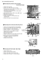
Removing the top cover (See Fig.1)

1. Remove 4 screws "A" on both sides of the top cover
    and 3 screws "B" on the rear side. 
2. Lift the back of the top cover spreading both sides
    to remove.


Removing the front panel assembly (See Fig.2,3)

1. Remove the top cover.
2. Remove 4 screws "C" on the bottom side and 3 screws
    "D" on the top side.
3. Disconnect the wire CN811 on the main board.
4. Disconnect the wire CN314 on the  audio & source
    selector board.
5. Remove the front panel assembly.


Removing the rear panel (See Fig.4)

1. Remove the top cover.
2. Remove 21 screws "E" on the rear panel. 
3. Remove 3 screws "F" on the rear panel. 
4. Remove the power cord stopper up side.
5. Remove the rear panel.


Removing the tuner board and 


video board (See Fig.5)

1. Remove the rear panel.
2. Remove 1 screw "G" on the video board
3. Disconnect the connector CN311 on the
    video board
4. Disconnect the connector CN111 on the
    audio & source selector board.

A   2

A   2

B

B

B

Fig.1

C

C

C

C

Fig.2

BOTTOM COVER

Fig.4

Power cord
Stopper

E

CN311

G

VIDEO board

Fig.5

Audio &
source
selector
board

Tuner
board

CN111

D

D

D

Fig.3

CN811

CN314

Main

board

Audio &
source
selector
board

F

F

F

E

E

E

E

Summary of Contents for RX-5000VBK

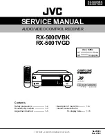
Page 1: ... RM SR558U REMOTE CONTROL TAPE MD FM AM VCR DVD SOUND CONTROL SLEEP 8 3 2 1 5 SURROUND TEST DELAY 6 5 4 EFFECT CENTER 5 9 8 7 P REAR L 5 TV VCR AUDIO CD 10 10 REAR R MENU ENT 5 TV CH TV VIDEO PHONO CD DISC TV VOL DVD MULTI ONE TOUCH OPERATION VCR CH MUTING VOLUME POWER RX 5000V AUDIO VIDEO CONTROL RECEIVER STANDBY PHONES SPEAKERS 1 2 ADJUST BASS BOOST SETTING MEMORY DVD MULTI CD DVD PHONO VCR TAPE...

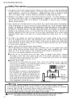
Page 2: ...akage currnet check Electrical shock hazard testing After re assembling the product always perform an isolation check on the exposed metal parts of the product antenna terminals knobs metal cabinet screw heads headphone jack control shafts etc to be sure the product is safe to operate without danger of electrical shock Do not use a line isolation transformer during this check Plug the AC line cord...

Page 3: ...ve the front panel assembly Removing the rear panel See Fig 4 1 Remove the top cover 2 Remove 21 screws E on the rear panel 3 Remove 3 screws F on the rear panel 4 Remove the power cord stopper up side 5 Remove the rear panel Removing the tuner board and video board See Fig 5 1 Remove the rear panel 2 Remove 1 screw G on the video board 3 Disconnect the connector CN311 on the video board 4 Disconn...

Page 4: ... 8 screws I on the main board 4 Remove 8 screws J on the power transistor 5 Disconnect the connector CN511 and wire CN831 on the main board 6 Each tie band is cut out 7 Remove 2 screws K on push switch of the front side 8 Remove nut on terminal of the headphone 9 The solder of the wire connected with the transformer is removed 10 Remove the main board Removing the front board See Fig 9 1 Remove th...

Page 5: ...efore adjustment If the heat sink is already warm from previous use the correct adjustment can not be made 3 For L ch connect a DC voltmeter between TP001 s pin1 and pin2 Lch And connect it between pin3 and pin4 Rch 4 30 minutes later after power on adjust VR741 for L ch or VR742 for R ch so that the DC voltmeter value has 1mV 10mV 1 Tuner range FM 87 5MHz 108 0MHz AM MW 530kHz 1710kHz VR742 TP001...

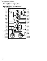
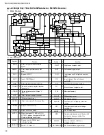
Page 6: ...2 OUT1 AVDD SWIN GNDS SRin SLin GNDC Cin GNDR Rin GNDL Lin BYPASSR BYPASSL LTRE LBASS3 LBASS2 LBASS1 DVDD CLK DATA LATCH DGND AGND SWout SRout SLout Cout Rout Lout AVSS CL1 CL2 CR1 CR2 RTRE RBASS3 RBASS2 RBASS1 OUT PUT PORT volume volume volume volume volume volume MCU I F tone tone 1 Block Diagram M62446FP IC341 6CH Master volume Description of major ICs ...

Page 7: ...nter volume signal input terminal Analog ground terminal R ch volume signal input terminal Analog ground terminal L ch volume signal input terminal Non connect Frequency adjustment terminal tone treble Frequency adjustment terminal tone bass Tone output terminal Frequency adjustment terminal tone bass Frequency adjustment terminal tone treble Frequency adjustment terminal tone bass L R volume inpu...

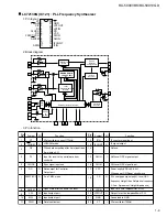
Page 8: ... BUFFER AM OSC REG AM RF AFC AM AGC O I O I I I AM Local oscillation Signal output This is a terminal of AM Local oscillation circuit Register value between pin 26 and pin28 besides the frequency width of the input signal AM RF signal input This is an output terminal of voltage for FM AFC This is an AGC voltage input terminal for AM O O I O AM detection output FM detection output Mpx input termina...

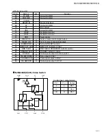
Page 9: ...Input output port Input output port Data input output Function IF counter signal input IF signal output Not use AM Local OSC signal output FM Local OSC signal input Power suplly VDD 4 5 5 5V When power ON Reset circuit move PLL charge pump output H Local OSC frequency Height than Reference frequency L Low Agreement Height impedance Input for active lowpassfilter of PLL Output for active lowpassfil...

Page 10: ...a signal output to DSP Inhibit detection signal input Clock signal input from RDS Data input from RDS Function switch data signal output Remote control signal input Data start signal for block data to output serial data Stereo indicator output Stereo L Mono H When the set is tuning this terminal becomes L Chip enable output to IC121 Clock signal for IC121 Function switch clock signal output Tuner ...

Page 11: ...ation terminal Oscillation terminal Power supply Center ch relay control signal output Front ch relay control signal output Surround ON OFF control INPUT ATT Indicator control ONE TOUCH OPERATION indicator control STANDBY indicator control Strobe signal output of function switch Data output to IC341 Clock signal output to IC341 Strobe signal output to IC341 I O O O O O O O O O O 2 Pin Function 2 2...

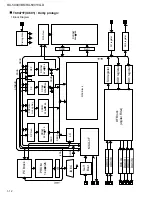
Page 12: ...US CRAM 320w 16b OFP CP DFRAM 64w 16b CRP Gen Lin Log Adj CROM 256w 16b DP Gen DRAM 256w 24b FBUS DBUS FBUS MAC Block SI0 register SO0 register SO1 register DF Block digital Filter MCU I F ADC L ADC R DAC L DAC R DAC C DAC S Self Boot IDEC LC IR PROM 1kw 32b PC Block JMP LDA LDB STABUS FBUS TC9471F IC601 Dolby prologic ...

Page 13: ...l output terminal R channel Ground terminal For DAC R channel Ground terminal For DAC C channel DAC analog signal output terminal C channel DAC analog signal output terminal with attenuator For C channel Reference voltage terminal For DAC C channel Power supply terminal For DAC C channel Reference voltage terminal for attenuator Output buffer Reference voltage terminal for attenuator Input buffer ...

Page 14: ... Operation flag output terminal MCU interface Acknowledge signal output terminal MCU interface Error flag output terminal MCU interface IC bus mode select terminal Self boot control terminal Non connect Power supply terminal Ground terminal Digital ground terminal For ADC L channel Analog ground terminal For ADC L channel ADC analog signal input terminal L channel Reference voltage terminal For AD...

Page 15: ...RX 5000VBK RX 5001VGD 1 15 Internal connections for FL display tube QLF0002 001 DI401 FL DISPLAY TUBE ...

Page 16: ...n Japan 200011 V VICTOR COMPANY OF JAPAN LIMITED AUDIO COMMUNICATION BUSINESS DIVISION PERSONAL MOBILE NETWORK BUSINESS UNIT 10 1 1Chome Ohwatari machi maebashi city 371 8543 Japan No 20883 RX 5000VBK RX 5001VGD ...

Reviews: