background image

SERVICE MANUAL

No. 86693

April 2002

SPECIFICATIONS 

DIGITAL  VIDEO  CAMERA

Printed in Japan

This service manual is printed on 100% recycled paper.

COPYRIGHT © 2002 VICTOR COMPANY OF JAPAN, LTD.

GR-DVL145EG

No. 86693

GR-DVL145EG

VICTOR COMPANY OF JAPAN, LIMITED
VIDEO DIVISION

S40894

(The specifications shown pertain specifically to the model GR-DVL145EG/EK)

Camcorder

General

Power supply

: DC 11.0 V

 (Using AC Adapter)

DC 7.2 V

 (Using battery pack)

Power consumption

LCD monitor off, viewfinder on

: Approx. 4.3 W

LCD monitor on, viewfinder off

: Approx. 5.3 W

Dimensions (W x H x D)

: 83 mm x 94 mm x 223 mm

(with the LCD monitor closed and the viewfinder
pushed down)

Weight

: Approx. 630 g

Operating temperature

: 0°C to 40°C

Operating humidity

: 35% to 80%

Storage temperature

: –20°C to 50°C

Pickup

: 1/4" CCD

Lens

: F 1.6, f = 3.9 mm to 62.4 mm, 16:1 power zoom lens

Filter diameter

: ø40.5 mm

LCD monitor

: 2.5" diagonally measured, LCD panel/TFT active

matrix system

Viewfinder

: Electronic viewfinder with 0.24" black/white LCD

Speaker

: Monaural

Digital Video Camera

Format

: DV format (SD mode)

Signal format

: PAL standard

Recording/Playback format

: Video: Digital component recording
: Audio: PCM digital recording, 32 kHz 4-channel

(12-bit), 48 kHz 2-channel (16-bit)

Cassette

: Mini DV cassette

Tape speed

: SP: 18.8 mm/s

LP: 12.5 mm/s

Maximum recording time

: SP: 80 min.

(using 80 min. cassette)

LP: 120 min.

Connectors

S-Video

Output

: Y: 1 V (p-p), 75 

, analogue

C: 0.29 V (p-p), 75 

, analogue

AV

Video output

: 1 V (p-p), 75 

, analogue

Audio output

: 300 mV (rms), 1 k

, analogue, stereo

DV

Output

: 4-pin, IEEE 1394 compliant

AC Adapter

Power requirement

: AC 110 V to 240 V

`

, 50 Hz/60 Hz

Output

: DC 11 V

, 1 A

Specifications shown are for SP mode unless otherwise indicated. E & O.E.
Design and specifications subject to change without notice.

Summary of Contents for GR-VF10EG

Page 1: ...Camcorder Allgemein Spannungsversorgung 11 V Gleichstrom bei Netzbetrieb 7 2 V Gleichstrom bei Batteriebetrieb Leistungsaufnahme Bei ausgeschaltetem LCD Monitor und eingeschaltetem Sucher Ca 4 3 W Bei eingeschaltetem LCD Monitor und ausgeschaltetem Sucher Ca 5 3 W Abmessungen B x H xT 83 mm x 94 mm x 223 mm bei eingeklapptem LCD Monitor und vollständig abgesenktem Sucher Gewicht Ca 630 g Umgebungs...

Page 2: ...L145EG X GR VF10EG NO ITEM FINAL ASSEMBLY M2 101 UPPER CASE ASSY LY20867 002A LY20867 002B 149 ZOOM UNIT LY20693 001B LY20693 005B 181 SPECIAL SCREW X2 LY30019 026A LY30019 026B REF MODEL GR DVL145EG X GR VF10EG NO ITEM MECHANISM ASSEMBLY M3 454 REEL DISK TAKE UP ASSY LY40443 002A LY40443 002B 468 DRUM ASSY YDV2086S CX YDV2086T CX 490 MECHA A ASSY YMA0025YJ REF MODEL GR DVL145EG X GR VF10EG NO ITE...

Page 3: ...Printed in Japan 0208WPC VICTOR COMPANY OF JAPAN LIMITED HOME AV NETWORK BUSINESS UNIT 12 3 chome Moriya cho kanagawa ku Yokohama kanagawa prefecture 221 8528 Japan ...

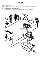
Page 4: ... are critical for safety Replace only with specified part numbers 5 1 PACKING AND ACCESSORY ASSEMBLY M1 The instruction manual to be provided with this product will differ according to the destination 5 6 2 1 31 30 3 FINAL ASSY M2 18 19 LABEL SERIAL 15 32 35 20 34 17 16 9 36 ...

Page 5: ... BOOK IT 9 BT 54013 4 WARRANTY CARD 15 QPA01703005 POLY BAG 16 QAM0212 001 CABLE ASSY AUDIO VIDEO CABLE 17 QQR0918 002 CORE FILTER 18 LY20847 001C AC ADAPTER AP V12EG 19 QQR0917 002 CORE FILTER 20 QMPL120 190 JR POWER CORD 30 LY32566 001A BATTERY PACK BN V408U 31 LY20186 001A SHOULDER STRAP 32 LY43606 001A LENS CAP ASSY 34 QQR0491 002 CORE FILTER 35 QAM0302 001 ADAPTER PLUG 36 MINI DV TAPE M DV60V...

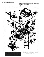
Page 6: ...5 444 447 463 424 421 420 425 416 415 428 427 422 AA AA AA 423 426 446 451 450 469 468 469 413 AA AA AA AA AA AA BB BB BB BB 482 481 482 5 2 MECHANISM ASSEMBLY M3 Classification Part No Symbol in drawing Grease KYODO SH JB AA Oil YTU94027 BB NOTE The section marked in AA and BB indicate lubrication and greasing areas BEWARE OF BOGUS PARTS Parts that do not meet specifications may cause trouble in ...

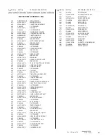
Page 7: ...42645 001A REEL DRIVE PULLEY ASSY 437 YQ44246 2 SLIT WASHER 438 LY40391 002B CENTER GEAR ASSY 439 LY40396 001A TIMING BELT 440 LY40413 001A COLLAR X2 441 LY31854 001A GUIDE ARM ASSY 442 LY31786 001A SLIDE GUIDE PLATE UNIT 443 YQ43893 2 MINI SCREW 444 LY42651 001B TENSION ARM ASSY 445 YQ44246 SLIT WASHER 446 LY30471 001D PAD ARM ASSY 447 YQ44246 SLIT WASHER 448 LY42745 001A IDLER ARM ASSY 449 YQ442...

Page 8: ...CD Lens F 1 6 f 3 9 mm to 62 4 mm 16 1 power zoom lens Filter diameter ø40 5 mm LCD monitor 2 5 diagonally measured LCD panel TFT active matrix system Viewfinder Electronic viewfinder with 0 24 black white LCD Speaker Monaural Digital Video Camera Format DV format SD mode Signal format PAL standard Recording Playback format Video Digital component recording Audio PCM digital recording 32 kHz 4 cha...

Page 9: ...M PHASE 2 15 2 6 MECHANISM ADJUSTMENTS 2 16 2 6 1 Assembling slide deck assembly and main deck assembly 2 16 2 6 2 Locating tension pole 2 17 2 7 SERVICE NOTE 2 18 2 8 COMPATIBILITY ADJUSTMENT 2 20 2 8 1 Jig connector cable connection 2 20 2 8 2 Tape pattern check 2 21 TABLE OF CONTENTS Section Title Page Section Title Page 3 ELECTRICAL ADJUSTMENT 3 1 PRECAUTION 3 1 3 2 SETUP 3 2 4 CHARTS AND DIAG...

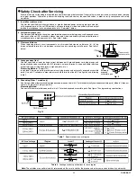
Page 10: ...e specified for compli ance with recognized codes pertaining to X ray emission Consequently when servicing these products replace the cath ode ray tubes and other parts with only the specified parts Under no circumstances attempt to modify these circuits Unauthorized modification can increase the high voltage value and cause X ray emission from the cathode ray tube 12 Crimp type wire connector In ...

Page 11: ... between terminals and surrounding metallic parts See table 1 below 4 Leakage current test Confirm specified or lower leakage current between earth ground power cord plug prongs and externally exposed accessible parts RF terminals antenna terminals video and audio input and output terminals microphone jacks earphone jacks etc Measuring Method Power ON Insert load Z between earth ground power cord ...

Page 12: ...sembly assembly parts 3 Indicates the number in the disassembly diagram 4 Indicates parts and points such as screws washers springs which must be removed during disassembly assembly Symbol Name Point S Screw L Lock Pawl Hook SD Soldering 夡 Others Connector Cover Bracket etc Example 2 S1 Remove the two screws S1 for removing the part 1 CN 2a Disconnect the connector 2a SD1 Unsolder at the point SD1...

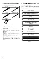
Page 13: ...system optical lens surface 1 3 DISASSEMBLY ASSEMBLY OF CABINET PARTS AND BOARD ASSEMBLY 1 3 1 Disassembly flow chart This flowchart indicates the disassembly step for the cabi net parts and board assembly in order to gain access to item s to be serviced When reassembling perform the step s in reverse order Table 1 2 1 Table 1 3 1 Torque driver YTU94088 1 Bit YTU94088 003 2 3 Chip IC replacement j...

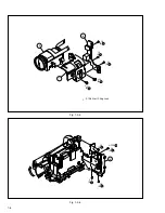
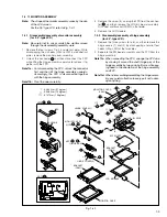
Page 14: ... any parts Particularly take care not to scratch or stain the lenses NOTE 8 As screw No 24 is hidden behind the cassette cover open the cassette cover to enable re moval of the screw NOTE 0a As the CN572 is located at the back of the as sembly unplug the three connectors and re move the screws before disconnecting the CN572 NOTE 0b Be careful not to damage any of the switches CONN No Pin No CONNEC...

Page 15: ...1 4 2 13 14 15 8 S 2 d 11 S 2 a CN 2 10 S 2 a 9 S 2 a 4 S 2 b NOTE CAP DC JACK 2 11 6 7 8 BOTTOM SIDE REAR SIDE 9 10 L 2 7 S 2 b 6 S 2 b 5 S 2 c 3 S 2 a Fig 1 3 1 1 1 S 1 a 2 S 1 b L 1 a L 1 b Fig 1 3 2 ...

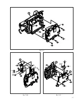
Page 16: ...1 5 Fig 1 3 3 3 NOTE a L 3 b 14 S 3 b CN 3 13 S 3 b 12 S 3 a L 3 a NOTE b 3 3 Fig 1 3 4 4 BRACKET OP ASSY CN 4 b CN 4 a CN 4 c 17 S 4 16 S 4 15 S 4 ...

Page 17: ...1 6 Fig 1 3 6 5 7 6 21 S 7 22 S 7 18 S 6 19 S 6 20 S 6 0 196 N m 2 0 kgf cm 8 8 NOTE CN 8 23 S 8 24 S 8 25 S 8 26 S 8 Fig 1 3 5 ...

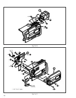
Page 18: ...31 S 9 b 30 S 9 b 27 S 9 a L 9 b CN 9 28 S 9 b Fig 1 3 8 Fig 1 3 9 NOTE a EJECT SW 10 32 S 10 33 S 10 CN 10 b CN 10 c CN 10 a CN 10 d 10 NOTE b 10 11 12 L 11 b 34 S 11 a 36 S 11 b 35 S 11 b L 11 a SHIELD PLATE CN 11 a CN 11 b CN 11 c ...

Page 19: ...b 43 S 14 b 41 S 14 a 40 S 14 a 39 S 14 a L 15 46 S 15 b 45 S 15 b 47 S 15 b 44 S 15 a COVER HINGE PLATE SPK SW 14 15 CN 14 0 147 N m 1 5 kgf cm NOTE 15 NOTE 14 Fig 1 3 10 13 38 S 13 b 37 S 13 a NOTE a NOTE b L 13 13 13 CN 13 ...

Page 20: ...embly DIF sheet and bracket FRM2 in that order 4 Remove the LCD module 1 4 2 Disassembly assembly of hinge assembly for 2 5 type LCD 1 Remove the three screws 6 to 8 and then remove the hinge covers 1 and 2 by disengaging a total of four hooks L g L h at the two sides 2 Separate the SW board assembly and the FPC from the hinge assembly Note c When connecting the FPC arrange the FPC wire by winding...

Page 21: ...ve the VF HINGE ASSY Note b Be careful not to damage the FPC and not to break any wires during the operation 0 078 N m 0 8 kgf cm 0 098 N m 1 0 kgf cm S a 1 EYE CUP CASE A VF 13 S b 4 13 L b 13 13 L c 13 L a 13 S c 5 13 S a 2 13 S d 8 13 S a 3 13 S c 6 13 S c 7 13 CASE B VF VF HINGE ASSY HOLDER LCD VF LENS ASSY FPC LEVER VF Note a 13 Note b SPRING VF CAP VF 5 Remove the screw 8 and the remove the ...

Page 22: ...sensor Note 5b When replacing the CCD image sensor don t re place it individually but replace the CCD base as sembly in whole with a new one 1 6 3 How to assemble CCD base assembly and CCD board assembly 1 Install the optical LPF with the spacer rubber attached to its CCD side in the OP block assembly Note 5c Pay careful attention to the orientation of the LPF 2 Set the CCD base assembly with care...

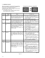
Page 23: ...s locked during mode shift 2 The mechanism is locked at the mechanism loading end because the encoder position is skipped during mechanism mode shift E03 TU SUP REEL FG In the case no REEL FG is produced for 4 sec onds or more in the capstan rotation mode af ter loading was complete the mechanism mode is shifted to STOP with the pinch roller set off This error is defined as E03 However no REEL EMG...

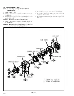
Page 24: ...rque Removing order of screw Place to stick screw Reference drawing Screw tightening torque Removing order of screw Place to stick screw Reference drawing Screw tightening torque 1 2 3 4 5 6 7 8 E VF ASSY B W Fig 1 5 1 IV VI IV II Removing order of screw Place to stick screw Reference drawing Screw tightening torque 1 2 3 4 5 6 7 8 5 OP BLOCK ASSY Fig 1 6 1 1 2 3 4 5 6 7 8 9 10 11 NOTE 1 Dont t re...

Page 25: ...olumn shows the side which the objective part is mounted on T the upper side B the lower side 4 Symbols appearing in this column indicate drawing numbers Step Part Name Fig Point Note Remarks 5 This column indicates parts and points such as screws washers springs and others to be removed fitted for disassembling reassembling the mechanism Besides such the parts this column occasionally indicates w...

Page 26: ...rical adjustment etc 9 Communication cable Connect the Communication cable between the PC ca ble and Jig connector cable when performing a PC ad justment 10 PC cable To be used to connect the VideoMovie and a personal computer with each other when a personal computer is used for adjustment 11 Service support system To be used for adjustment with a personal computer 12 Alignment tape To be used for...

Page 27: ...Fig 2 3 3 Fig 2 3 4 Fig 2 3 5 Fig 2 3 6 Fig 2 3 7 Motor DC3V EJECT mode Back side of deck C IN mode EJECT mode STOP mode SHORT FF mode PLAY mode REV mode SUB CAM GEAR TOP VIEW BOTTOM VIEW Fig 2 3 8 2 3 2 Explanation of mechanism mode The mechanism mode of this model is classified into six modes as shown in Table 2 3 1 Each mechanism mode can be distinguished from others by the relative position of...

Page 28: ...E SUP LOADING SUB BRAKE T PINCH ROLLER BRAKE PAD ARM TENSION 0 0 0 EJECT C IN 30 31 7 33 70 74 04 77 SHORT FF STOP 169 2 160 176 REV 211 5 200 220 PLAY 280 3 265 291 5 43 1 45 6 47 4 46 8 49 5 51 5 122 5 129 5 134 7 156 6 148 1 162 9 44 6 47 2 49 1 49 2 52 0 54 1 161 7 155 5 147 0 250 5 265 0 275 6 SLIDE START SLIDE END ROTARY ENCODER 3 2 1 2 3 3 Mechanism timing chart ...

Page 29: ...art 1 Configuration 2 Procedures for disassembly A Mechanism assembly Main deck assembly Slide deck assembly Mechanism assembly Main deck assembly Slide deck assembly Cassette housing assembly Cassette housing assembly B C A B C 2a 5b 7a 8a 11e 7h Fig 2 4 1 Fig 2 4 2 ...

Page 30: ...ke assembly T Fig 2 4 11 W7 L7a P7a 7e Adjustment 7b Guide pin S T S7a 7c Pad arm assembly T W7 L7b P7b 7d 7d Slide guide plate assembly T S7b 7c Adjustment 7e Collar T 7a 7f Collar T 7a 7g Sub brake assembly T W7 L7c P7c 7b 7h Control plate assembly T 2 W7 L7d P7d 7b C Main deck assembly 8a Tension lever assembly T Fig 2 4 12 8c 8b Slide lever assembly T 8b 8c Brake control lever assembly T 8a 9a...

Page 31: ... 3a 7c 2a 7b 7a 7d 7e 9c 3c 3b 7h 2b 9f 8a 10c 9e 5b 9d 5a 4c 4a 4b 11b 11a CMain deck assembly BSlide deck assembly 10e 3d 9a 2c 3e 9b 8c 7f 7g TOP VIEW BOTTOM VIEW 11e 11d 11c 8b 10b CMain deck assembly BSlide deck assembly 10a ...

Page 32: ...deformation in the frame or no damage to the switches etc Note 1d After reassembling the com ponent parts check the mechanism operation in the PLAY mode For details of checking method refer to 2 6 1 as sembling slide deck assem bly and main deck assem bly STOP mode EJECT mode PLAY mode Note 2a When removing the reel disk assembly be careful not to break the brake pad which applies lateral pressure...

Page 33: ...embly to the mechanism as the pad arm assembly is moved to the extent in the di rection of the arrow Note 4a When removing the cleaner arm assembly it is recom mended to remove the slant pole arm assembly together with it except the case of a single unit replacement because the hook L4a is hard to disengage Note 4b How to set the coil spring P4b 3 3a Tension arm assembly 3b Release guide assembly ...

Page 34: ...er deforma tion nor damage observed in them Note 5d When removing the rail assembly check to see if the collar is securely set in the arm groove Note 6a When removing the slide deck assembly pay heed to the three components of the following because they are apt to come off after the slide deck assembly is removed 8a Tension lever assembly 8b Slide lever assembly 8c Brake control lever assembly For...

Page 35: ...For details of reassembling procedure refer to 2 6 1 Assembling slide deck assembly and main deck as sembly Note 7d The pad arm assembly controls the tension level of the tension arm assembly For adjustment of the tension arm assembly refer to 2 6 2 Locating tension pole Note 7e When reinstalling the load brake assembly slightly lift the slide deck assembly upwards because the lower part of the lo...

Page 36: ...rake control plate 10c Rotary encoder 10d Connect gear 10e Reel drive pulley assembly Note 10a When removing refitting parts pay careful attention to the flexible board and so on not to damage them Note 10b When reinstalling the main cam gear and the brake control plate first fit them together so that the protrusion on the brake control plate is set in the slot on the main cam gear as shown below ...

Page 37: ... S11 W11 23 S11 11d 11c 11b 11a Fig 2 4 15 11 11a Catcher T assembly 11b Capstan motor 11c Charge arm assembly 11d Sub cam gear 11e PWB holder Note 11 The following figure shows how to put the charge arm as sembly and sub cam gear assembly together 11d 11c ...

Page 38: ...7 P7c P4a P4b 20 S11 21 S11 17 S10 15 S9 16 S10 12 S9 22 S11 24 S11 5 S2a 4 S2a 6 S2b 11 S7b 10 S7a 23 S11 7 S4 8 S4 13 S9 Cassette housing assembly CMain deck assembly 1 S1 L1b L1d L1c L1a A BSlide deck assembly 3c 9b 9c 10e 10d 9e 10c 8a 9f 10b 10a 8b 11a 11b 4a 4b 9a 3e 8c 11d 11e 7g 7a 2a 7d 7h 2b 2c 3d 3b 3a 7c 7b 11c 4c 5a 9d 5b 7f 7e Note Classification Part No Symbol in drawing Grease KYOD...

Page 39: ... gear Set the sub cam gear so that its locating hole meets the hole on the main deck assembly This state represents that the mechanism is in the EJECT mode which is the mechanism assembly mode Connect gear Note 2 Set the connect gear so that its locating hole meets the hole on the main deck assembly Note 1 Note 1 Since the connect gear 2 is tightly fixed to the main deck by caulking adjust its pha...

Page 40: ...to 2 3 2 Explanation of mechanism mode 3 Press the end face B of the slide deck assembly reel disk side and the end face C of the main deck assem bly drum assembly side with uniform force so that the two assemblies are tightly pressed to each other Further more press the part D and tighten the screw A Note Tightening torque for screw A 0 069 N m 0 7 kgf cm 3 2 3 3 1 3 3 C C D A B B œ Œ ...

Page 41: ...er the mechanism assembly into the PLAY mode Refer to 2 3 2 Explanation of mechanism mode 2 When the part is positioned down make sure that the part a of the tension arm assembly is located within the range of b 3 If the part a is out of the range turn the pin c to adjust the position ...

Page 42: ...e assembly W3b 1 Idler arm assembly W3a 1 Pinch roller arm assembly Guide arm assembly Cleaner arm assembly W4 1 P4a 1 P4b 1 Slant pole arm assembly S4 3 Drum assembly Guide roller S assembly W5a 3 W5b 1 Rail assembly 2a 2b 3a 3b 3c 3d 3e 2c 4b 5b 4a 5a 4c 2 7 SERVICE NOTE Use the following chart to manage mechanism parts that are removed for disassembling the mechanism Table 2 7 1a ...

Page 43: ...ion lever assembly Slide lever assembly Brake control lever assembly Loading guide Timing belt Center gear assembly S9 2 Motor bracket assembly W9 1 Worm wheel S9 1 Gear holder Main cam gear Brake control plate S10 1 W10a 1 W6 1 Rotary encoder W10a 1 Connect gear W10b 1 Reel drive pulley assembly Catcher T assembly S11 2 Capstan motor W11 1 Charge arm assembly S11 1 Sub cam gear S11 2 PWB holder 7...

Page 44: ...nnector cable schematic diagram 20 20 AL_3VSYS 19 18 17 16 15 14 13 12 11 10 9 8 7 6 5 4 3 2 1 LABEL MAIN CN105 JIG BOARD PIN NO DISCRI 10 19 DRST VPPD 9 18 SRV_RX JLIP_RX 8 17 JLIP_TX GND 7 16 HID1 PB_CLK 6 15 ENV_OUT MAIN_VCO 5 14 ATFI FS_PLL 4 13 I_MTR IF_TX 3 12 CJIG_RST SRV_TX 2 11 REG_3V VPPC AL_3VSYS DRST SRV_RX JLIP_TX HID1 ENV_OUT ATFI I_MTR CJIG_RST REG_3V DISCRI VPPD JLIP_RX GND PB_CLK ...

Page 45: ...n the tape has been played back again Moreover perform readjustment as required 6 When the recording has been played back again play back the self recording to confirm that the waveform is flat Fig 2 8 3 Fig 2 8 4 Fig 2 8 5 CN105 ENV_OUT CN105 HID1 Flatten the waveform Misalignment of guide roller height on the take up side Misalignment of guide roller height on the supply side NOTE The plate serv...

Page 46: ...ragile carefully handle them in dis connecting and connecting 3 Shortcircuit between operation and DECK chassis 2 Required test equipment 1 Color TV monitor 2 AC adapter 3 Oscilloscope dual trace type observable 100 MHz or higher frequency Note It is recommended to use one observable 300 MHz or higher frequency 4 Digital voltmeter 5 Frequency counter with threshold level adjuster 6 Personal comput...

Page 47: ... Remove one screw 1 first and the cover JIG next Fig 3 2 1 Connection for Service support system 9 Alignment tape To be used for check and adjustment of interchange ability of the mechanism 10 INF adjustment lens To be used for adjustment of the camera system 11 INF adjustment lens holder To be used together with the camera stand for operat ing the VideoMovie in the stripped down condition such as...

Page 48: ...mm 16 1 power zoom lens Filter diameter ø40 5 mm LCD monitor 2 5 diagonally measured LCD panel TFT active matrix system Viewfinder Electronic viewfinder with 0 24 black white LCD Speaker Monaural Digital Video Camera Format DV format SD mode Signal format PAL standard Recording Playback format Video Digital component recording Audio PCM digital recording 32 kHz 4 channel 12 bit 48 kHz 2 channel 16...

Page 49: ...s are the same PB mode REC mode 4 Voltage measurement 1 Regulator DC DC CONV circuits REC Colour bar signal PB Alignment tape Colour bar Unmeasurable or unnecessary to measure 4 Indication on schematic diagram Voltage Indications for REC and PB mode on the sche matic diagram are as shown below 5 Signal path Symbols The arrows indicate the signal path as follows NOTE The arrow is DVC unique object ...

Page 50: ...m component face parts face indicated 2 Parts location guides Parts location are indicated by guide scale on the circuit board Note For general information in service manual please refer to the Service Manual of GENERAL INFORMA TION Edition 4 No 82054D January 1994 LOCATION REF No IC101 B C 6 A IC Category IC Horizontal A zone Vertical 6 zone B Foil side A Component side C Chip component D Discret...

Page 51: ...OSD_HD BUS 0 15 OSD_VD DOT_CLK VC 0 3 CAM_VD CLK4M5 MVD CALE OMT MFLD MFLD OUTH OUTV TMS TDO DYI 0 3 MVD DCI 0 3 INV DCO 0 3 INH DYO 0 3 S_SHUT REG_3V GND S_DET EJT_SW CAS_SW CLK_OUT DATA_OUT TG_RST DRWSEL DRE DWE DALE TG_CS SRV_RDY SRV_CS S_CLK S_DT_OUT SRV_RST PBPLLCTL PBPLLCTL GND CCD C_FG Vdd HG_BS C_FG HG_U HG_W HG_W JACK Page 4 37 HG_U HG_V HG_V LOAD_REV GND C_COIL_U C_COIL_U C_COIL_W C_COIL...

Page 52: ...NS SREELLED MIC3 MIC2 MIC1 GND D_PFG COIL_COM D_COIL_W D_COIL_W D_COIL_V D_COIL_V D_COIL_U D_COIL_U D_PG D_FG LOAD_REV GND DEW_SENS LOAD_REV LOAD_FWD LOAD_FWD EJT_SW C_FG HG_BS C_FG HG_U HG_W HG_W HG_U HG_V HG_V GND C_COIL_U C_COIL_U C_COIL_W C_COIL_W C_COIL_V C_COIL_V REG_3V HG_BS GND REG_4 8V BL_GND GND REG_3V KEY_A AV_GND GND LITHIUM IR_RMC SPK SPK VDCVF HDCVF VF_LCD GND LCD_G VFREG4 8 REG_12V ...

Page 53: ...D_TBC_IN OSD_TBC_OUT OSD_TBC_CLK TBC_CS BZ_FREQ BZ_ENV A_CSYNC TBC_RST EXT_IN_L S_IN_L TGFZ_RST TG_CS CDS_CS CCD_CTL REV_SW LCD_RST VDD VSS M_RVS VF_LCD LCD_CTL VF_CTL FLSH_RST REG_CS LAMP_ON NC CHRG_WKUP AVREF_OFF DIAL_PB DIAL_OFF DIAL_AUTO DIAL_MANU A_FADE CHRG_EVR PHOTO_SW FOCUS_SW P_MEDIA NC F Z_CS IRIS_O C VPP XT1 RESET XT2 VDD OSCO OSCI VSS AUDIO_CS A_MUTE PWDA1 PWDA2 PWAD1 PWAD2 MD_DEM1 VDD...

Page 54: ... DIN_L NC XI164SEL VDD VSS REEL_ON MONI_CHG CLK27SEL FFREWH DV_RST NC NC NC NC NC NC NC NC CAP_REF DRUM_REF KENTO1_REF KENTO2_REF NC NC NC NC VPP XT1 RESET XT2 VDD OSCO OSCI VSS NC HID PBH RECH NC NC NC NC VDD VSS NC NC NC NC NC NC MSELECT NC NC NC DRUM_FG DRUM_PG NC OUTV NC NC VDD VSS T_REEL S_REEL TSR FRP NC NC NC NC SPA SRVTRK DRUM_FG CAP_FG NC NC NC NC S_SENS E_SENS DEW_SENS BCID1 BCID2 BCID3 ...

Page 55: ...TL1619 0 0082 12K 330P 0 01 0 047 39K 0 22 0 22 0 047 0 022 100K 1K 1 120k 680 0 47 10 100k 4 7K 0 1 390 0 33 0 01 0 0022 0 0022 0 0022 10 470 470 10K 10K 10K 10 0 0015 180 180 1K 1K 68K 68K 270 560K 10 0 0 150K 10K 4 7K 0 47 0 047 FGND1 D U D V D W D GND N C L FWD FGND2 L GND L REV C GND L UNREG C U C V C W N C C VM C UNREG C HW C HW C HV C HV C HU C HU C FGSOUT C FGOUT C FG C FG VCC C VS C PCV C...

Page 56: ...22 0 022 1 8k 1 8k 0 001 0 001 1 100k 0 1 1 4 7k 220k 0 1 2 7 2 7 0 1 0 1 4 7k 4 7k 4 7k 4 7k 15k 4 7k 15k 15k 2 2k 0 022 15k 2 2k 0 022 0Ω 0Ω 0Ω 0 01 0 01 0 1 1 AK4560AVQ 6 3 6 3 2SC4617 QR X INT_MIC L INT_MIC R IM_GND 6 3 6 3 6 3 6 3 UMX1N W 2SC4617 QR X T T T T T T Lch Rch ALC AMP ALC AMP Lch Rch MIX MIX MIX INT EXT EXT INT Control Register I F Audio I F Controller Clock Divider OFF OFF HPF A D...

Page 57: ...EFCLK ADVIN1 ADAVD1 ADAVS1 ADVRH1 ADVRL1 VSS PWM27O VDDE OSC27I OSC27O CLK27I CLK27O CLK27SEL VSS CLK135O VDDI FRRES FRREF TRKREF SERVOFRREF SERVOTRKREF PHYTPA PHYTPB PHYTPBIAS PHYXTPA PHYXTPB PHYRO PHYRF PHYFIL XRESET PHYVDA PHYVDR PHYVSA PHYVSR PHYAVS3 VDDE N C VDDE VSS PWMAUDIO VDDE VSSP VCIAUD VDDP VCXO11I VCXO11O VCXO12I VCXO12O OSC24I OSC24O OSC11I OSC11O DILRCK DIBCK DIMCK DIDAT AILRCK AIBC...

Page 58: ...2X 6 3 GND P R_GND GND P R_GND GND P R_GND GND P R_GND 2S 2F 1S 1F T T T PB_MONI DCS_C3 DCS_C2 DCS_C1 R_CTL VCC5 REC_H PB_H HID1 HID2 HID3 VDD2 8 DUMP PBIN_R HEAD_GND HEAD_GND HEAD_GND DX3 X3 Y3 DY3 HEAD_GND DX2 X2 Y2 DY2 HEAD_GND DX1 X1 Y1 DY1 HEAD_GND PB_OUT AGC_IN AGC_CTL AGC_DET PB_GND AGC_OUT AGC_BUFF_IN REG_1 1V AGC_BUFF_OUT VRB_AGC MAIN_GND ATF_GAIN VCA_OUT ATF_IN VRB_ATF ATF_OUT ATF_GND TC...

Page 59: ...220 240 240 220 150p 100p 33p 33p 0 01 4 7k 4 7k 330 1 10k 12k 10µ 10 68 68 68 560 560 10k 0 01 0 01 0 1 UMT2N W BA7665FS X 4 CH 4 UMZ1N W 6 3 T TO REG TO SYSCON TO DSP V OUT MAIN 0 1 75Ω 75Ω 6dB 75Ω 6dB 20k Mute Chroma Mute 6dB NOTE The parts with marked is not used y30160001a_rev0 TO MAIN IF CN103 TO MAIN IF CN103 TO REG When ordering parts be sure to order according to the Part Number indicated...

Page 60: ...Y_OUT R Y_OUT IREFC VREFC C_OUT IREFY VREFY Y_OUT Y2_OUT NC PBLK RE RW WE DSTB ALE ASTB BUS15 BUS14 BUS13 BUS12 BUS11 BUS10 BUS9 BUS8 BUS7 BUS6 BUS5 BUS4 BUS3 BUS2 BUS1 BUS0 CLR VDCPU HDCPU FRP OMT AFBEND FLDCPU BEND VSS GT_X VPD CS GT_S TDOUT TDIN TRST TMS TCK CPUSEL1 CPUSEL0 TVSEL DSCI7 DSCI6 DSCI5 DSCI4 VDDI VDMDA PWM CLK45 CLKOSD HDOSD VDOSD BLK1 BLK2 VC1 VC2 VR VG VB VBLK DSYI0 DSYI1 DSYI2 DS...

Page 61: ... DA_R DA_G DA_B REG_4 8V REG_3V GND VF_LCD 10µ 10 0 01 0Ω 12K 12K 12K 10µ 0 01 4 7 0Ω 270 270 270 9p 9p 9p 10k 0 01 1k 3 3k 22k 1M 1 1M 0 1 22K 3 3k 12k 22K 3 3k 22K 1 1 10k 10k 10k 10k 10k 10k 6 3 25 PUMX1 W TC7W53FU X PUMX1 W PUMX1 W PUMX1 W T T T CVF LCD NOTE The parts with marked is not used 0 1 MAIN MONI IF TO REG TO DSP TO REG TO SYSCON TO REG MQR0129 002X TO REG TO MAIN IF CN101 y30171001a_...

Page 62: ...000p 0 1 10 1 8K 22K 10 0 01 0 01 0 1 10 1k 10µ 0 1 10µ 1k 0 1 10µ 100k 0 1 1k 0 270 0 1k 6R8 6R8 6R8 6R8 10µ 1k 0 1K 22k 150k 10 33k 4 7K 100K 1M 0 1 4 7k 1M 24k 0 1 330k 0 01 0 1 100k 10k 10K 100k 68k 1 5k 0 01 22K 0 1 0 1 330 10k 1 10 0 1 2SC4617 RS X BA10358F XE EXP2 EXTb GND Cosc FILa FILb FILc FILd Vref Vdd Vm3 D2 FBd D1 Vm4 C2 FBc C1 EXP0 EXP1 RESET OSCout OSCin SCLK SDATA LATCH VD B2 FBb B...

Page 63: ...SSGCTL Vdd1 VGAT DSGAT HCLR RG Vss1 Vdd2 H1 Vdd3 H2 Vss3 Vdd4 SHP SHD XRS DCC Vss4 CAM VTR TEST Vdd5 CLK SSK CS SEN CLK27 CL1716 Vss5 XAHD XAVD WEN ID Vdd6 RST VM VH SUB VL Vss6 CLPDM CLK13 CL CLK18 MCK V2 V4 V1 V3 JCY0117 35 4 SUB H2 H1 RG GND GND GND GND GND GND GND GND V1 V2 V3 V4 NC GND OUT VDD NAX0356 001X 1SS355 X NQR0129 002X NQR0129 002X NQR0129 002X 20 10 CCD 7 0V CCD 15V CCD 15V T T T T ...

Page 64: ...k 47k 560p 10k 33k 1k 0 001 100k 10k 750 10k 33k 1k 0 1 1 0 1 220µ 0 1 1 18k 1 0 1 82k 1 100k 2 7k 100k 82k 1 1k 12k 1 560p 22k 82k 22µ 47k 100k 8 2k 68k 1 0 01 27k 47k 18k 100k 0 01 100k 220k RB480Y W IN7 IN7 FB7 IN8 IN8 FB8 IN1 FB1 IN2 FB2 IN3 FB3 IN6 FB6 IN4 IN4 FB4 IN5 IN5 FB5 CT GND RT CP VDRV CSS4 CSS5 CSS1 CSS2 CSS3 SHUTDOWN IN11 FB10 IN10 OUT10 PGND1 OUT7P OUT7N OUT1 OUT2 OUT3 OUT6 OUT4 OU...

Page 65: ... VD_OUT HD_OUT VDB_IN QH_SEL CPH_SEL HD_IN SYNC_IN DGND DVDD PN1 HPOS1 HPOS2 HPOS3 HPOS4 WH HDOT1 RESET AGND VCOI AVDD VCOO QVD PD POSSET JUST HDOT2 CPH1 RL CPH2 STV2 CPH3 MN5814 NQL085J 4R7X REV_SW BL_GND BL_GND LCD_CTL BL_4 8V BL_4 8V A_REG_3V VGL VSS STV2 UD CPV OEV STV1 VDD VGH LCD_COM LCD_VEE STH2 LCD_RVS VB MON_R MON_G MON_B GND GND CLK3 NC QGF0508F1 33X BA4558F X CLK2 CLK1 Q2H OEH STH1 UDZS...

Page 66: ...2 LCD_VDD VGH LCD_COM LCD_VEE STH2 LCD_RVS VB MON_R MON_G MON_B GND GND CLK3 CLK2 CLK1 Q2H OEH STH1 NMFZ007 R40X K 2SC4617 QR X NC EL EL VCC ENB GND RT2 RT1 CIL DC NQS0048 001X 6 2SD1664 QR W 2SD1664 QR W DTA144EE X R G B T T T TO LCD MODULE TO BACK LIGHT TO_EL TO MONITOR CN764 y30162001a_rev0 NOTE The parts with marked is not used 0 3 LCD BL N C TL503 TL7504 Exchange Prats List With EL MODEL With...

Page 67: ...ev0 DRUM MOTOR TO SENSOR TO LOADING MOTOR TO TO MAIN IF CN113 CHARGE LAMP TO DSP CN107 TO TG CN107 When ordering parts be sure to order according to the Part Number indicated in the Parts List For the destination of each signal and further line connections that are cut off from this diagram refer to 4 1 BOARD INTERCONNECTIONS NOTES IC5001 is incorporated in the CCD base assembly When IC5001 needs ...

Page 68: ... RPM7138 V4 NQR0251 004X 10 QNS0078 001 RPM 22P8 W B SENS MA8068 X MA8068 X QND0004 001 6 3 NQR0251 004X MA8068 X T T T T AV_GND GND AV JACK OUT IR_RMC Y_OUT Vcc JACK GND S_DET C_OUT GND IR_OUT REG_4 8V IR_AMP V_OUT AU_SIG L AU_SIG R P_DET AV_GND GND AV_GND GND AV_GND GND AV_GND GND AV_GND GND GND GND 0 6 NOTE The parts with marked is not used VEE Vcc TO MAIN IF CN103 y40098001a_rev0 S OUT When or...

Page 69: ...PL HCK RENE RENO VIDL VIDLC VIDCH BLACK_LEVEL NC VDD_CAP NC OK GAMMA HOLD_INV_F NC NC VDDH TEST SEL_PDR VBAT A_VBAT H_SYNC V_SYNC VHIO_SEL REF_GND VBG MCVVQ111FB GND VIDLO RENON RENEN HCLKN HPLN VREF BW_VDD BW_VEE BW_COM HLTOR HODL VPLN VIDHI VCKN PDR TCL NC NC NC QGF0517F2 20X NSCW100A0 ST X PUMX1 W VFREG4 8V REG_12V REG_4 8V LCD_Y SLEEP GND QGF0517F1 06X MA111 X 6 3 16 GAIN R7004 VF NTSC PAL 0 D...

Page 70: ...14 TL1415 TL1416 TL1417 TL1418 TL1419 TL3001 TL4201 TL4202 R3068 R3069 TL3005 R1610 R1611 R3057 R1083 R1619 R1620 R1621 R1624 R1628 R1003 R1006 R1637 R1009 R1014 R1015 R1018 R1022 R1027 R1028 R1039 R1049 R1050 R1066 R1071 R1072 C1601 R1013 C1618 C1619 C1620 C1029 C1030 C1034 C1037 C1627 C1013 C1020 C1021 Q1001 Q1005 Q1008 Q1009 IC1004 RA1008 IC1006 R1403 R1406 R1407 R1409 R1410 R1411 R1412 R1413 R...

Page 71: ...C4336 B C 3B C4337 B C 4C C4338 B C 4C C4339 B C 4B C4340 B C 4C C4341 B C 3C C4342 B C 4C C4343 B C 4C C4344 B C 3C C4345 B C 3C C4346 B C 3C C4347 B C 3B C4348 B C 3C C4349 B C 3B C4350 B C 4B C4360 B C 4A C4361 B C 4A C4366 B C 4A C4367 B C 4A C4369 B C 4A C4370 B C 4A C4371 B C 4A C4372 B C 4A C4373 B C 4A C4374 B C 4A C4375 B C 4B C4376 B C 4B C4377 B C 4B C4378 B C 4B C4379 B C 4A C4380 B C ...

Page 72: ...R4307 B C 5B R4308 B C 4B R4309 B C 5B R4310 B C 5B R4311 B C 4B R4312 B C 4B R4313 B C 4B R4314 B C 4B R4315 B C 4B R4333 B C 3B R4334 B C 3B R4335 B C 3B R4336 B C 3B R4337 B C 4B R4338 B C 4C R4339 B C 3B R4340 B C 3B R4341 B C 3B R4342 B C 4B R4343 B C 4B R4344 B C 4B R4345 B C 3C R4346 B C 4C R4347 B C 4B R4348 B C 4B R4349 B C 4B R4350 B C 4B R4351 B C 4B R4360 B C 4B R4361 B C 4A R4362 B C ...

Page 73: ...02 R3503 R3504 R3505 R3506 R3507 R3508 R3509 C3505 C3507 C3508 C3509 C3510 C3511 C3513 C3514 C3515 C3518 C3519 C3521 C3523 C3512 C3522 C3525 L3501 L3502 L3504 L3505 R1625 R1626 IC3501 R3521 R3522 S CASE S CASE L1 S CASE L2 C3527 L3503 R2006 R2009 R2014 R2015 R2016 R2017 C1006 C2013 R2018 C2014 R2019 R2020 RA1010 IC1002 R2023 X1002 R2028 R2101 R2102 R2103 CN107 CN108 CN104 R2108 R2110 R2112 R2113 R...

Page 74: ... A C 2B C7624 A C 3B C7625 A C 2C C7626 A C 3B C7627 A C 3B C7629 A C 2C C7630 A C 2B C7631 B C 1A C7632 A C 3B C7633 A C 3D C7634 A C 4B C7635 A C 3D C7636 A C 2C C7637 A C 2C C7638 A C 2C CONNECTOR CN761 B C 3D CN762 B C 1A CN763 B C 4A CN764 B C 2C DIODE D7601 A C 3D D7602 A C 2C D7603 A C 3C IC IC7601 A C 3C IC7602 A C 2D IC7603 A C 3B IC7604 A C 3C IC7605 A C 3B COIL L7601 A C 3D L7602 A C 2C...

Page 75: ...4 ZP2 19 ZP2 20 ZP2 21 ZP1 1 ZP1 3 ZP1 15 TL7501 TL7502 ZP1 25 ZP1 27 ZP1 28 ZP1 29 R7501 R7502 R7503 R7506 R7507 R7509 C7504 C7506 C7509 F7501 C7508 C7505 Q7503 Q7504 Q7505 Q7506 Q7501 Q7502 IC7501 CN751 L7503 C7505P R7511 T L 7 5 0 4 1 32 1 24 1 2 4 5 1 8 FOIL SIDE B COMPONENT SIDE A 0 3 LCD BL PWB YB20929 01 01 0 3 LCD BL PWB YB20929 01 01 ...

Page 76: ... CCD PWB YB20924 0 5 JUNCTION PWB YB20925 01 01 0 5 JUNCTION PWB YB20925 01 01 FOIL SIDE B COMPONENT SIDE A FOIL SIDE B COMPONENT SIDE A CCD VF FOIL SIDE B COMPONENT SIDE A JUNCTION L7002 C7005 CN7002 1 6 25 36 37 48 1 12 13 24 20 1 R7002 R7004 R7005 R7009 R7010 R7011 R7012 R7013 C7004 C7007 C7008 C7009 C7010 C7012 C7014 C7015 C7017 D7001 R7001 ZP1 6 ZP1 5 ZP1 4 ZP1 3 ZP1 2 ZP1 1 ZP2 17 C7006 IC70...

Page 77: ...502 C507 C509 R501 R507 R528 C502 C503 C501 CN502 J501 J503 R511 R513 R526 C505 C508 C514 L501 L503 C506 D501 D502 D503 D504 TL503 R502 R503 R504 R505 R506 R508 R509 C504 IC501 IC502 Q501 3 1 4 5 1 8 1 20 0 6 JACK PWB YB20925 01 01 0 6 JACK PWB YB20925 01 01 FOIL SIDE B COMPONENT SIDE A ...

Page 78: ...4 0 4 55 0 0 56 0 8 0 8 57 0 8 0 8 58 0 8 0 8 59 0 8 0 8 60 1 2 1 1 61 0 4 0 4 62 0 0 63 11 1 11 1 64 1 7 1 7 IC1602 1 2 3 1 3 1 3 4 0 0 5 6 0 0 7 8 3 1 3 1 Q1601 1 E 0 0 2 B 0 0 3 E 4 8 4 8 4 C 0 0 5 C 4 8 4 8 AUDIO MODE REC PLAY PIN NO IC2001 1 2 1 0 7 2 2 0 0 3 2 0 0 4 2 1 0 5 1 5 1 5 6 1 5 1 5 7 1 5 1 5 8 0 0 9 3 1 3 1 10 0 7 1 5 11 0 7 1 5 12 0 7 1 5 13 0 7 1 5 14 1 5 1 5 15 1 5 1 5 16 0 6 1 ...

Page 79: ...REG 12V M_REG4 8 REG_15V VFREG4 8 REG_4 8V REG4 8 Q6205 VF VCC1 L6101 IC6101 1 8V REG Q6203 REG 3V Q6201 L6102 F6101 PWR Q6210 CAPSTAN Q6208 DRUM PWR REG_2 5V REG_3V REG_1 8V REG 2 5V Q6202 CAP_PWR DRUM_PWR M_UNREG 10 9 2 3 GND GND BATT_ BATT_ 10 9 CN104 2 3 REG 0 1 MAIN M_UNREG DET IC3005 Q3002 IC3001 DVMAIN MONI IF AUDIO Q2002 IC1006 Q1002 IC1003 IC1008 IC2001 SPK SPK DRUM_PWR REG_4 8V REG_3V 15...

Page 80: ..._STS 19 MXDT_OUT 165 DSC_CLK 17 FLSH_RST 167 100 DSC_DT_OUT 2 174 0 CN721 CN763 6 4 12 BW Y LCD_Y CN764 25 24 23 CN751 24 0 3 23 22 MON_R MON_G 0 8 B W VF CN722 MONITOR 2 DIN3 DIN0 DIN4 4 57 7 135 3 134 38 37 34 WCLK DIN11 WXAD WE 39 132 203 48 130 IC4302 FILED MEMORY 32 15 19 DO0 IE DO3 199 49 198 21 31 8 9 DO4 DO11 RCLK RXAD 261 257 203 200 LCD MODULE CN752 17 16 15 B G R 10 13 RE RAE1 201 50 c ...

Page 81: ...BUFF_OUT 10 REC_GAIN ATF_GAIN 60 ATF_GAIN 57 PB_MONI MONI_CHG REC_DTA REC_CTL 12 44 7 MONI_CHG R_CTL REC_DATA REC_CLK 9 REC_CLK Y1 19 X2 25 X1 20 1F 2S 1S RECCTL RECDATA RECCLK FSPLLCTL TO D CPU HID1 RECH PBH HID3 HID3 40 42 41 HID1 REC_H PB_H 38 Y2 24 IC3501 2F 2 1F 7 3 6 2S 1S CN110 2F HEAD DAAOUT0 DAAOUT1 DISCRI CLK27SEL OSC27I OSC27O PWM27O 11 237 106 IC3005 AMP AMP AMPO 4 1 2 2 4 IC3502 A0 A1...

Page 82: ...N1 IN11 23 50 48 IN2 25 OUT3 56 IN3 27 OUT6 55 IN6 29 OUT10 62 IN10 63 34 Q6208 L6206 C6215 Q6210 L6207 C6218 C6221 AL3V SW REG REG_2 5V REG_3V REG_3V REG_3V M_UNREG 2 5V SW REG CN105 11 REG_3V CN101 22 CN109 15 37 M_REG4 8V 27 26 M_REG4 8 CN101 M_REG4 8 9 8 L6204 CN103 2 Q6212 Q6213 REG_12V 28 REG_12V CN101 33 31 Q6215 Q6216 D6206 Q6205 Q6206 VFREG4 8 CN101 REG_15V REG CCD D_GAIN REG4 8 REG_ 15V ...

Page 83: ...Printed in Japan VICTOR COMPANY OF JAPAN LIMITED VIDEO DIVISION S40894 ...

Page 84: ...T BOOK PO C LYT1023 014A INST BOOK HU C 9 BT 54013 2 WARRANTY CARD 15 QPA01703005 POLY BAG 16 QAM0212 001 CABLE ASSY AUDIO VIDEO CABLE 17 QQR0918 002 CORE FILTER 18 LY20847 001C AC ADAPTER AP V12EG 19 QQR0917 002 CORE FILTER 20 QMPL120 190 JR POWER CORD 30 LY32566 001A BATTERY PACK BN V408U 31 LY20186 001A SHOULDER STRAP 32 LY43606 001A LENS CAP ASSY 34 QQR0491 002 CORE FILTER 35 QAM0302 001 ADAPT...

Page 85: ...9 145C 145A 145 145B 160 160 162 158A 164 162 165 162 161 158B 158C 161 158 159 163 163 e d c b a 157 161 155 152 153 154 150 146A 150 149 151 146 151 166 167 167 182 184 181 183 181 184 184 188 q 168 168 168 167 s kk t 167 167 MAIN 01 JACK 06 MECHANISM M3 JUNCTION 05 k e v a c h g f r j m cc m k y b d j hh n y z p p n hh u r gg gg g h jj u jj s t v w x w aa aa x z kk ee dd ee 204 251C 251C 251C 2...

Page 86: ...EW 149 LY20693 001B ZOOM UNIT 150 LY30018 096A SPECIAL SCREW X2 151 LY30018 084A SPECIAL SCREW X2 152 LY20575 004B GRIP BELT 153 LY42891 001A HOOK GRIP 154 LY30018 0D1A SPECIAL SCREW 155 LY32093 001B COVER ZOOM ASSY 156 LY30018 092A SPECIAL SCREW 157 LY30018 065A SPECIAL SCREW 158 LY20697 001D ARM ASSY 158A LY30001 023A TENSION SPRING 158B LY30029 0C7A SPACER A 158C LY30029 0E9A SPACER A 159 LY300...

Page 87: ...3 411 410 411 411 411 409 432 435 433 434 430 429 441 461 460 457 459 458 443 442 453 455 454 465 464 465 466 467 452 457 456 471 471 482 470 431 473 474 401 478 472 462 440 440 445 444 447 463 424 421 420 425 416 415 428 427 422 AA AA AA 423 426 446 451 450 469 468 469 413 AA AA AA AA AA AA BB BB BB BB 482 481 482 BEWARE OF BOGUS PARTS Parts that do not meet specifications may cause trouble in re...

Page 88: ... BRAKE CONTROL LEVER ASSY 436 LY42645 001A REEL DRIVE PULLEY ASSY 437 YQ44246 2 SLIT WASHER 438 LY40391 002B CENTER GEAR ASSY 439 LY40396 001A TIMING BELT 440 LY40413 001A COLLAR X2 441 LY31854 001A GUIDE ARM ASSY 442 LY31786 001A SLIDE GUIDE PLATE UNIT 443 YQ43893 2 MINI SCREW 444 LY42651 001B TENSION ARM ASSY 445 YQ44246 SLIT WASHER 446 LY30471 001D PAD ARM ASSY 447 YQ44246 SLIT WASHER 448 LY427...

Page 89: ...LDER LED 339 LY43239 001A GUIDE VF X2 340 LY30018 060A SPECIAL SCREW X4 341 LY30029 0U6A SPACER A 342 LY43489 001B PLATE VF ELECTRONIC VIEWFINDER ASSEMBLY M4 301 LY32349 001A EYE CUP 302 LY20766 001A CASE A VF 304 LY32351 001A CAP VF 305 LY20768 001A VF HINGE ASSY 306 QLD0193 001 LCD MODULE 307 QAL0380 002 FPC 309 LY30018 0F1A SPECIAL SCREW X3 312 LY41701 002A SHEET CAUTION 1 314 LY43041 002A LABE...

Page 90: ...ART No PART NAME DESCRIPTION 505 QYSPSPT1730R SCREW X2 506 LY30018 0F2A SPECIAL SCREW X2 507 LY32574 001A MONITOR FPC ASSY 508 QLD0234 001 LCD MODULE 509 LY32079 001A HINGE ASSY 510 LY32088 001A HINGE COVER 1 511 LY32089 001B HINGE COVER 2 512 QYSPSPT1730R SCREW 513 LY30018 058A SPECIAL SCREW X2 514 LY30018 023A SPECIAL SCREW 515 LY43392 001A LIGHT SCREEN 516 QLL0125 001 LAMP 517 LY43778 001A HOLD...

Page 91: ...GI TRANSISTOR or PDTA114EE DIGI TRANSISTOR or RN2102 DIGI TRANSISTOR or UN9111J DIGI TRANSISTOR Q1402 UMC3N DIGI TRANSISTOR Q1403 UMC3N DIGI TRANSISTOR Q1601 UMC3N DIGI TRANSISTOR Q2001 UMX1N PAIR TRANSISTOR Q2002 2SC4617 RS X TRANSISTOR Q2004 2SC4617 RS X TRANSISTOR Q3001 2SC4617 RS X TRANSISTOR Q3002 2SC4617 RS X TRANSISTOR Q3701 UMT2N PAIR TRANSISTOR or XP6401 TRANSISTOR Q3702 UMZ1N PAIR TRANSI...

Page 92: ... 103W MG RESISTOR 10kØ 1 16W R1082 NRSA6AJ 103W MG RESISTOR 10kØ 1 16W R1083 NRSA6AJ 103W MG RESISTOR 10kØ 1 16W R1090 NRSA6AJ 474W MG RESISTOR 470kØ 1 16W R1091 NRSA6AJ 474W MG RESISTOR 470kØ 1 16W R1092 NRSA6AJ 154W MG RESISTOR 150kØ 1 16W R1093 NRSA6AJ 154W MG RESISTOR 150kØ 1 16W R1094 NRSA6AJ 474W MG RESISTOR 470kØ 1 16W R1095 NRSA6AJ 474W MG RESISTOR 470kØ 1 16W R1096 NRSA6AJ 154W MG RESISTO...

Page 93: ...W R3033 NRSA6AJ 103W MG RESISTOR 10kØ 1 16W R3034 NRSA6AJ 222W MG RESISTOR 2 2kØ 1 16W R3036 NRSA6AJ 103W MG RESISTOR 10kØ 1 16W R3037 NRSA6AJ 681W MG RESISTOR 680Ø 1 16W R3050 NRSA6AJ 0R0W MG RESISTOR 0Ø 1 16W R3051 NRSA6AJ 0R0W MG RESISTOR 0Ø 1 16W R3057 NRSA6AJ 100W MG RESISTOR 10Ø 1 16W R3059 NRSA6AJ 101W MG RESISTOR 100Ø 1 16W R3066 NRSA6AJ 561W MG RESISTOR 560Ø 1 16W R3067 NRSA6AJ 561W MG RE...

Page 94: ...ESISTOR 1 8kØ 1 16W R4916 NRSA6AJ 102W MG RESISTOR 1kØ 1 16W R4917 NRSA6AJ 102W MG RESISTOR 1kØ 1 16W R4918 NRSA6AJ 0R0W MG RESISTOR 0Ø 1 16W R5501 NRSA6AJ 0R0W MG RESISTOR 0Ø 1 16W R5503 NRSA6AJ 270W MG RESISTOR 27Ø 1 16W R5504 NRSA6AJ 270W MG RESISTOR 27Ø 1 16W R5505 NRSA6AJ 270W MG RESISTOR 27Ø 1 16W R5506 NRSA6AJ 0R0W MG RESISTOR 0Ø 1 16W R5507 NRSA6AJ 0R0W MG RESISTOR 0Ø 1 16W R5509 NRSA6AJ 4...

Page 95: ...C1410 NCBA1CK 103W CAPACITOR 0 01µF 16V C1411 NCBA1CK 103W CAPACITOR 0 01µF 16V C1412 NCBA1CK 223W CAPACITOR 0 022µF 16V C1413 NCBA1CK 223W CAPACITOR 0 022µF 16V C1414 NCBA1CK 223W CAPACITOR 0 022µF 16V C1415 NCBA1CK 223W CAPACITOR 0 022µF 16V C1416 NCBA1AK 104W CAPACITOR 0 1µF 10V C1601 NCBA1CK 103W CAPACITOR 0 01µF 16V C1602 NBE20JM 106X T CAPACITOR 10µF 6 3V C1603 NBE20JM 106X T CAPACITOR 10µF ...

Page 96: ...04W CAPACITOR 0 1µF 10V C3511 NCBA1CK 103W CAPACITOR 0 01µF 16V C3512 NCB31CK 104X CAPACITOR 0 1µF 16V C3513 NCBA1AK 104W CAPACITOR 0 1µF 10V C3514 NCBA1AK 473W CAPACITOR 0 047µF 10V C3515 NCBA1AK 473W CAPACITOR 0 047µF 10V C3516 NCBA1AK 473W CAPACITOR 0 047µF 10V C3517 NCBA1CK 103W CAPACITOR 0 01µF 16V C3518 NCBA1CK 103W CAPACITOR 0 01µF 16V C3519 NCBA1HK 102W CAPACITOR 0 001µF 50V C3520 NCBA1CK ...

Page 97: ...AM 106X T CAPACITOR 10µF 10V C4917 NBE21AM 106X T CAPACITOR 10µF 10V C4918 NCBA1AK 104W CAPACITOR 0 1µF 10V C4919 NCFA1AZ 104W CAPACITOR 0 1µF 10V C4920 NCBA1AK 104W CAPACITOR 0 1µF 10V C5501 NCBA1AK 104W CAPACITOR 0 1µF 10V C5503 NCBA1AK 104W CAPACITOR 0 1µF 10V C5504 NCBA1AK 104W CAPACITOR 0 1µF 10V C5505 NCBA1AK 104W CAPACITOR 0 1µF 10V C5506 NBE40GM 476X T CAPACITOR 47µF 4 0V C5507 NCBA1AK 104...

Page 98: ...QR0129 002X FERRITE BEAD L4903 NQL315K 100X COIL 10µH L5501 NQL315K 100X COIL 10µH L5502 NQR0129 002X FERRITE BEAD L5503 NQR0129 002X FERRITE BEAD L5504 NQR0129 002X FERRITE BEAD L5505 NQL315K 100X COIL 10µH L5506 NQL315K 100X COIL 10µH L6101 NQLZ011 4R7X COIL 4 7µH L6102 NQLZ011 4R7X COIL 4 7µH L6201 NQL52EM 390X COIL 39µH L6202 NQL52EM 390X COIL 39µH L6203 NQL52EM 390X COIL 39µH L6204 NQL144K 22...

Page 99: ...6X T CAPACITOR 10µF 16V C7610 NDC31HJ 330X CAPACITOR 33pF 50V C7611 NCB31EK 103X CAPACITOR 0 01µF 25V C7612 NCB31EK 103X CAPACITOR 0 01µF 25V C7613 NCB31EK 103X CAPACITOR 0 01µF 25V C7614 NCB21CK 334X CAPACITOR 0 33µF 16V C7615 NDC31HJ 331X CAPACITOR 330pF 50V C7616 NDC31HJ 560X CAPACITOR 56pF 50V C7617 NDC31HJ 220X CAPACITOR 22pF 50V C7618 NCB31EK 103X CAPACITOR 0 01µF 25V C7619 NDC31HJ 270X CAPA...

Page 100: ... 0Ø 1 16W C501 NBE21AM 335X T CAPACITOR 3 3µF 10V C502 NCF31CZ 104X CAPACITOR 0 1µF 16V C503 NCB31EK 153X CAPACITOR 0 015µF 25V C504 NCB31EK 153X CAPACITOR 0 015µF 25V C506 NBE21AM 106X T CAPACITOR 10µF 10V C509 NBE20JM 226X T CAPACITOR 22µF 6 3V C514 NCB31HK 103X CAPACITOR 0 01µF 50V C515 NCB31HK 103X CAPACITOR 0 01µF 50V L501 NQR0251 004X FERRITE BEAD L502 NQR0251 004X FERRITE BEAD L503 NQR0251 ...

Reviews: