D
C
B
A
4
5
3
2
1
D
C
B
A
4
5
3
2
1
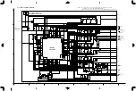
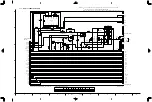
4-36
4-35
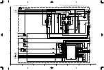
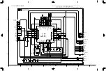
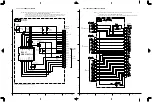
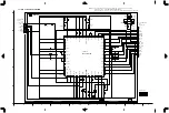
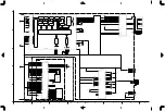
CCD SCHEMATIC DIAGRAM
4.17
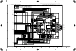
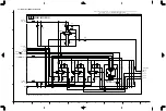
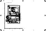
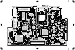
JUNCTION SCHEMATIC DIAGRAM
4.18
IC5001
C5001
C5010
C5008
Q5001
R5001
R5005
C5007
CN5001
C5006
C5005
C5004
L5001
C5002
C5009
C5003
R5003
0.1
0.01
4.7K
1M
1000p
0.1
0.1
10
10
µ
2.2
0.1
100K
MN39160FH-J
2SC3931/CD/-X
/16
/35
T
T
CCD -7.0V
SUB
H1
H2
RG
GND
GND
GND
GND
GND
GND
GND
CCD OUT
V4
V3
V2
V1
CCD +15V
CCD +15V
NC
SUB
H1
H2
RG
V4
V3
V2
V1
GND
GND
Vdd
V
out
TEST
VL
∗
∗
NOTE : The parts with marked ( ) is not used.
∗
0 4 CCD
TO TG
CN107
y40099001a_rev0
y40069001a_rev0
DRUM MOTOR
TO
SENSOR
TO
LOADING MOTOR
TO
TO MAIN IF
CN113
CHARGE LAMP
TO DSP
CN107
TO TG
CN107
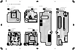
When ordering parts, be sure to order according to the Part Number indicated in the Parts List.
For the destination of each signal and further line connections that are cut off from
this diagram, refer to "4.1 BOARD INTERCONNECTIONS".
NOTES :
IC5001 is incorporated in the CCD base assembly. When IC5001 needs replacement, replace
the CCD base assembly in whole because it cannot be re-placed alone.
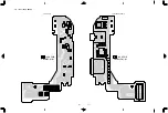
When ordering parts, be sure to order according to the Part Number indicated in the Parts List.
For the destination of each signal and further line connections that are cut off from
this diagram, refer to "4.1 BOARD INTERCONNECTIONS".
NOTES :


