2-39
2-40
CONTRE LES RISQUE D'INCENDE,
DE MEME TYPE ET DE MEME TENSION.
REMPLACER LES FUSIBLES PAR UN AUTRE
POUR UNE PROTECTION PERMANENTE
CAUTION:
FOR CONTINUED PROTECTION AGAINST
FIRE HAZARD ,REPLACE ONLY WITH SAME
TYPE AND RATED FUSE(S).
ATTENTION:
TM2
CN9013
IC105
CN13
L3502
C5204
C5216
L7001
TL9002 TL9013
TL9014
R156
L6701
R6019
C1630
TL1601
R173
CN1
CN5
C4033
CN7
C4034
R105
R108
R110
R111
R112
R113
R115
R116
R118
R119
R125
R126
R128
R129
R130
C4035
R138
R139
R141
R146
R149
R154
R166
R132
R1605
R1607
R1608
R2072
R2403
R4020
R4022
R4021
R4019
R4034
R4035
R159
R6804
R4025
R4014
L2072
R3506
R3903
R176
D9401
D9402
R5202
C5220
C5221
C5224
R4203
R4204
R4206
R4207
R4208
R4209
TL9003
R4215
R4216
R4218
R4219
R4221
R4224
R4516
R4505
R3501
R4703
R4704
R180
R4709
R4710
RA9101
TM1
R6024
IC6002
R6103
R6104
R6105
R6203
R6204
R6304
TM3
F7301
L7301
R6606
R6614
R6812
R9602
R9604
TL9004
TL101
R7007
R7005
R7009
R7011
R7002
R7014
R7301
Q7302
R9116
R6803
R7310
R7311
R7312
R7313
C9406
L9402
C9405
L9401
R123
R1601
TL102
C1623
C104
C107
C110
C115
C121
C124
C125
C129
C136
C1205
C1610
ZPPTLOPENSW
TL1602
TL1603
Q9101
C2072
C2404
C4029
C4030
C4028
C4036
R4225
C3510
C3511
C3901
C3903
C4027
C4018
CN9012
C4012
Q9102
C4048
R174
C4037
C5223
R5221
C4202
C4207
C4701
C4212
ZP4-2
C6105
C6110
C6205
C6210
C6610
ZP4-1
ZP6-2
IC5202
1
1
1
1
18
11
14
10
11
20
CN22
ZP25-19
C3509
ZP8-1
ZP8-2
ZP16-9
ZP12-3
C6705
ZP13-3
C4211
ZP18-6
ZP25-8
L5203
C1607
C1614
C1615
C1616
C1618
ZP13-11
ZP13-12
ZP13-13
C4045
ZP25-7
C4209
ZP27-1
ZP27-2
C2402
C6802
ZP12-1
C6811
ZP28-8
ZP33-16
ZP18-4
TL5202
ZP101-1
R5212
TL5203
ZP18-5
ZP18-8
ZP25-13
ZP13-4
ZP16-5
ZP13-1
ZP18-12
ZP101-2
R6018
C2403
C5203
R9104
ZP-CCD1
ZP25-14
ZP31-2
C111
C112
C2401
C4251
C4256
R9102
C6002
ZP-CCD2
Q101
C9407
Q4701
Q4702
R9402
R9403
Q6002
Q6003
TL115
Q6702
ZP33-14
Q7001
Q7002
Q7003
D4001
Q9103
D102
Q9104
R1625
R1626
RA107
RA108
RA109
RA110
R1627
R1628
IC1602
CN3
CN2
CN18
IC1801
CN8
CN27
Q4251
IC103
1
4
5
8
TM4
CN25
C7009
R7019
J505
CN4
TL1619
Q115
R181
R182
C6803
R6014
C6022
C6023
C6008
R6016
X101
CN12
R6707
R6708
R6709
R190
L6301
L6601
R4032
R135
R103
L6401
L6501
C2029
R104
R106
R107
R109
R114
R117
R122
R127
R140
R142
R143
R144
R145
R147
R155
R164
R165
R168
R170
R158
R148
R131
R1606
R1615
R1616
R175
R2401
R2402
L2071
R4033
R3901
R3902
R169
C106
ZPPCN15
R5218
R4027
R4028
R4029
R4030
R4031
R4201
R4202
CN15
R4217
R4220
R4222
R4223
R4258
R4262
R4701
R4707
R6314
L6101
L6201
D6001
R6303
R6305
R6704
R9603
R6715
R7001
R7004
R7010
R172
CN16
R7003
R7006
R7008
R7012
R7016
R161
Q7303
C7302
C7303
R102
R124
R179
C102
C101
C137
L5205
L5206
C4043
C113
C114
C123
C127
C131
C133
C134
C140
C130
C1201
C1608
C4032
IC4202
1
1
7
8
14
13
Q4202
C4025
C3513
C3515
C3902
C6703
C4046
C4038
C4039
C4040
C4041
C4042
R177
C5222
C5225
R5220
C5206
C5226
C4203
R178
C4206
C4208
R1620
C1624
C4702
C4703
C4716
C4717
C6305
C6310
C7002
C7005
R137
C128
C1617
C1619
C3514
L5204
C4210
C6004
C3512
C4026
C7008
C7006
C7007
L2401
C109
C1609
C7001
C108
C1202
C1206
C4201
C6303
C6307
C6203
Q102
Q103
Q105
L6302
Q2401
Q4001
Q4201
Q4501
C4047
Q7301
C117
Q106
Q6811
Q3901
C9320
D103
D104
D5201
D101
C4008
CN9031
R7018
IC4003
1
10
11
20
IC2401
1
4
5
8
IC1601
1
16
17
32
33
48
49
64
IC101
1
44
45
88
89
132
133
176
R5217
X4001
C7010
J504
CN6
R7020
C7011
Q114
C4513
C5231
R6011
R6013
C6019
R6007
Q110
Q111
1
14
1
10
11
20
1
20
1
1
1
14
16
1
11
1
10
1
10
1
25
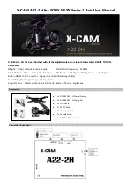
MAIN CIRCUIT BOARD
4
3
G
F
E
D
C
B
A
COMPONENT SIDE (A)
<01>MAIN YB10400-01-03
2
1
Summary of Contents for GR-AX880US
Page 35: ...1 26 No 86721 ...