CH-X550
1-30 (No.49787)
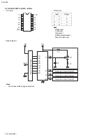
4.4 HD74HC126FP-X (IC651) : Buffer
• Pin layout
• Pin function
Note:
H:High level
L:Low level
X:Irrelevant
Z:Off(High-impedance)
State a 3-state input
• Block diagram
Note:
CL includes probe and jig capacitance
1
2
3
4
5
6
7
1C
1A
1Y
2C
2A
2Y
GND
VCC
4C
4A
4Y
3C
3A
3Y
14
13
12
11
10
9
8
Input
Output
C
A
Y
L
X
Z
H
L
H
H
H
L
Vcc
Vcc
Input
See Function
Table
1A
2A
3A
4A
1C
2C
3C
4C
1Y
2Y
3Y
4Y
Output
Output
Output
Output
Sample as Load Circuit 1
Sample as Load Circuit 1
Sample as Load Circuit 1
1k
1k
S1
CL

