CH-X550
1-28 (No.49787)
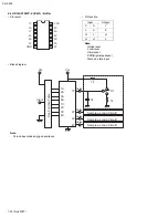
4.2 BR24C01AF-W-X (IC604) : EEPROM
• Pin layout
• Pin function
• Block diagram
Vcc
WP SCL SDA
A0
A1
A2 GND
Symbol
I/O
Description
Vcc
-
Power supply
GND
-
GND
A0, A1, A2
I
Slave address setting terminal
SCL
I
Serial clock input terminal
SDA
I/O Slave/word address serial data input/output
WP
I
Write protect terminal
A0 1
A1 2
A2 3
GND 4
8 Vcc
7 WP
6 SCL
5 SDA
1kbit EEPROM
7bit
7bit
8bit
Address
decoder
Slave/Word
Address register
Data
register
Control circuit
High voltage circuit
Voltage detection
START
STOP
ACK

