REL1.0
Page 1 of 80
Zynq Ult MPSoC SOM Hardware User Guide
iWave Systems Technologies Pvt. Ltd.
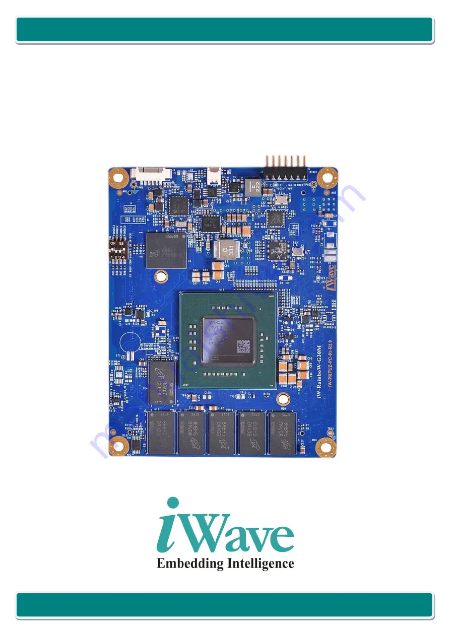
iW-RainboW-G30M
Zynq Ult MPSoC SOM
Hardware User Guide
Page 1: ...REL1 0 Page 1 of 80 Zynq Ultrascale MPSoC SOM Hardware User Guide iWave Systems Technologies Pvt Ltd iW RainboW G30M Zynq Ultrascale MPSoC SOM Hardware User Guide...
Page 2: ...ntains proprietary material for the sole use of the intended recipient s Do not read this document if you are not the intended recipient Any review use distribution or disclosure by others is strictly...
Page 3: ...n errata and associated issues Trademarks All registered trademarks product names mentioned in this publication are the property of their respective owners and used for identification purposes only Ce...
Page 4: ...3 6 MPSoC System Monitor ADC 20 2 4 PMIC with RTC 20 2 5 Memory 21 2 5 1 DDR4 SDRAM with ECC for PS 21 2 5 2 DDR4 SDRAM for PL 21 2 5 3 eMMC Flash 21 2 6 On SOM Fearures 22 2 6 1 JTAG Header 22 2 6 2...
Page 5: ...Zynq Ultrascale MPSoC PS Pin Multiplexing on Board to Board Connectors 68 3 TECHNICAL SPECIFICATION 70 3 1 Electrical Characteristics 70 3 1 1 Power Input Requirement 70 3 1 2 Power Input Sequencing...
Page 6: ...PSoC SOM Top View 75 Figure 12 Mechanical dimension of Zynq Ultrascale MPSoC SOM Bottom View 76 Figure 13 Mechanical dimension of Zynq Ultrascale MPSoC SOM Side View 76 Figure 14 Zynq Ultrascale MPSoC...
Page 7: ...igh speed ruggedized terminal strip connectors provide the carrier board interface to carry all the I O signals to and from the Ultrascale MPSoC SOM 1 3 List of Acronyms The following acronyms will be...
Page 8: ...PL Programmable Logic PS Processing System RGMII Reduced Gigabit Media Independent Interface RTC Real Time Clock SD Secure Digital SDIO Secure Digital Input Output SGMII Serial Gigabit Media Independ...
Page 9: ...ctor Signal LVDS Low Voltage Differential Signal GBE Gigabit Ethernet Media Dependent Interface differential pair signals USB Universal Serial Bus differential pair signals OD Open Drain Signal OC Ope...
Page 10: ...SE 16ADC 4 Bank 45 Bank 46 Bank 64 FPGA IOs 22SE 8ADC 4 FPGA IOs 24SE 12ADC 4 High Speed Transceiver 4 Channels 2 High Speed Transceiver 4 Channels 2 GTH Transceiver FPGA IOs GTH Transceiver FPGA IOs...
Page 11: ...y FBVB900 ZU7EG ZU5EG ZU4EG Programming Logic with up to 504K Logic cells and Processing System with integrated Quad core ARM Cortex A53 MPCore Application processor up to 1 5GHz Dual core ARM Cortex...
Page 12: ...E IOs o Upto 3 HDGC Global Clock Input pins LVDS SE o Upto 8 ADC Input pins Differential Single Ended PL IOs HD Bank462 Upto 12 LVDS IOs 24 Single Ended SE IOs o Upto 4 HDGC Global Clock Input pins LV...
Page 13: ...IOs HP Bank662 Upto 24 LVDS IOs 48 Single ended SE IOs o Upto 4 GC Global Clock Input pins LVDS SE o Upto 16 ADC Input pins Differential Single Ended General Specification Power Supply 5V from Board...
Page 14: ...The Zynq Ultrascale MPSoC SOM is based on Xilinx Zynq Ultrascale MPSoC with FBVB900 package Zynq Ultrascale MPSoC family integrates Processing system PS and Xilinx programmable logic PL in a single de...
Page 15: ...e Zynq Ultrascale MPSoC s PS has 78 dedicated I O pins referred as MIO Multiplexed I O for the PS peripheral interfaces These 78 MIO pins are divided into three banks PS BANK500 501 502 and each bank...
Page 16: ...s of 24pins In Zynq Ultrascale MPSoC PL each bank supports four global clock GC or HDGC input pin pairs GC pins have direct access to the global clock buffers MMCMs and PLLs of the same Bank HDGC pins...
Page 17: ...ltrascale MPSoC SOM Reference Clock Sl No On SOM Oscillator Frequency SoC Ball Name Pin Number Signal Type Termination Description 1 33 33MHz PS_REF_CLK P19 1 8V LVCMOS 33 33Mhz single ended reference...
Page 18: ...he boot device to the on chip RAM The FSBL initiates the boot of the PS and can load and configure the PL or configuration of the PL can be deferred to a later stage The Zynq Ultrascale MPSoC SOM supp...
Page 19: ...n device reset MPSoC mode pins are read to determine the primary boot device The Zynq Ultrascale MPSoC SOM supports Boot Mode switch SW1 to select the required boot device By default eMMC is supported...
Page 20: ...uses 10 bit 1MSPS ADC to digitize the sensor inputs It is located in the PS LPD and monitors two temperature points several internal fixed voltage nodes The PS has two temperature sensors one is phys...
Page 21: ...This device operates at 1 2 voltage level In Zynq Ultrascale MPSoC SOM Bank65 is used for PL DDR4 interface The RAM size can be expandable up to maximum of 4GB based on the availability of higher den...
Page 22: ...evel JTAG interface signals are also connected to Board to Board Connector2 to access from carrier board Internally the Zynq Ultrascale MPSoC implements both an ARM debug access port DAP inside PS as...
Page 23: ...Power Supply Voltage 3 GND Power Ground 4 PS_JTAG_TMS PS_JTAG_TMS L21 I 1 8V LVCMOS 4 7K PU JTAG Test Mode Select 5 GND Power Ground 6 PS_JTAG_TCK PS_JTAG_TCK L19 I 1 8V LVCMOS 4 7K PU JTAG Test Clock...
Page 24: ...SoC device which can be used to fix the heatsink Fan if required The Fan Header J2 is physically located on topside of the SOM as shown below Number of Pins 2 Connector Part 0530480210 from Molex Mati...
Page 25: ...faces of Zynq Ultrascale MPSoC to the carrier board by adding these two Board to Board Connectors The Zynq Ultrascale MPSoC SOM Board to Board Connector1 pinout is provided in the below table and the...
Page 26: ...S45_L12N 29 30 PL_L15_LVDS45_L1P PL_D16_LVDS45_L9P 31 32 PL_K15_LVDS45_L2P PL_C16_LVDS45_L9N 33 34 PL_K14_LVDS45_L2N GND 35 36 GND GTHTXP2_223 37 38 PL_J16_LVDS45_L4P GTHTXN2_223 39 40 PL_H16_LVDS45_L...
Page 27: ...4 105 106 NC GND 107 108 NC GTHRXN1_224 109 110 NC GTHRXP1_224 111 112 NC GND 113 114 GND GTHRXN0_224 115 116 PL_F13_LVDS46_L5N_HDGC GTHRXP0_224 117 118 PL_G13_LVDS46_L5P_HDGC GND 119 120 GND Key Key...
Page 28: ...USB1_CLK PS_MIO 64_502 GTHTXN1_225 191 192 GEM3_TXD0 USB1_DIR PS_MIO65 _502 GND 193 194 GEM3_TXD1 USB1_DATA2 PS_MIO 66_502 GTHRXN1_225 195 196 GEM3_TXD2 USB1_NXT PS_MIO67 _502 GTHRXP1_225 197 198 GEM...
Page 29: ...nal Name B2B 1 Pin B2B 1 Pin Signal Name GTHTXN3_225 225 226 GEM3_RXD1 USB1_DATA4 PS_MIO 72_502 GND 227 228 GEM3_RXD2 USB1_DATA5 PS_MIO 73_502 GTHRXN3_225 229 230 GEM3_RXD3 USB1_DATA6 PS_MIO 74_502 GT...
Page 30: ...channels at 1 25Gb s The available peripheral standard option for each PS GTR transceiver lane in Zynq Ultrascale MPSoC is shown below This is user programmable via the high speed I O multiplexer HS...
Page 31: ...ial transmitter negative 175 PS_MGTRRXN1_505 PS_MGTRRXN1_505 J30 I DIFF PS GTR Lane1 High speed differential receiver negative 177 PS_MGTRRXP1_505 PS_MGTRRXP1_505 J29 I DIFF PS GTR Lane1 High speed di...
Page 32: ...1_NX T PS_MIO67_502 PS_MIO67_502 C28 O 1 8V LVCMOS GEM3 RGMII Transmit DATA2 Or USB1 ULPI NXT 198 GEM3_TXD3 USB1_DA TA0 PS_MIO68_502 PS_MIO68_502 C29 O 1 8V LVCMOS GEM3 RGMII Transmit DATA3 Or USB1 UL...
Page 33: ...ed on these pins the same pins can be used as GPIOs or other alternate functions Please refer PS Min Multiplexing section 2 9 for available alternate functions For more details on CAN Interface pinout...
Page 34: ...k inputs Bank 226 on Board to Board Connector2 In Zynq Ultrascale MPSoC SOM On board reference clock to the GTH transceiver quad is not supported This must be fed from the carrier board based on the p...
Page 35: ...HRXP2_223 MGTHRXP2_223 T2 I DIFF GTH Bank223 channel2 High speed differential receiver positive 43 GTHTXP3_223 MGTHTXP3_223 R4 O DIFF GTH Bank223 channel3 High speed differential transmitter positive...
Page 36: ...HRXP2_224 MGTHRXP2_224 K2 I DIFF GTH Bank224 channel2 High speed differential receiver positive 129 GTHTXP3_224 MGTHTXP3_224 K6 O DIFF GTH Bank224 channel3 High speed differential transmitter positive...
Page 37: ...ank225 channel2 High speed differential transmitter negative 235 GTHRXN2_225 MGTHRXN2_225 F1 I DIFF GTH Bank225 channel2 High speed differential receiver negative 237 GTHRXP2_225 MGTHRXP2_225 F2 I DIF...
Page 38: ...nput capable pins of PL Bank45 Also Board to Board Connector1 pins 12 14 18 16 27 28 29 30 31 32 33 34 38 40 42 44 are PLSYSMON auxiliary analog Input capable pins of PL Bank45 Note In ZU7CG 7EG 7EV M...
Page 39: ...r Single ended I O 29 PL_A15_LVDS45_L12N IO_L12N_AD8N_45 A15 IO 1 8V LVDS PL Bank45 IO12 differential negative Same pin can be configured as PLSYSMON differential analog input8 negative or Single ende...
Page 40: ...I O 44 PL_J15_LVDS45_L3P IO_L3P_AD13P_45 J15 IO 1 8V LVDS PL Bank45 IO3 differential positive Same pin can be configured as PLSYSMON differential analog input13 positive or Single ended I O 56 PL_D17_...
Page 41: ...able pins of PL Bank46 Also Board to Board Connector1 pins 46 48 50 52 70 72 74 76 87 88 89 90 91 92 93 94 116 118 124 126 130 132 142 144 are PLSYSMON auxiliary analog Input capable pins of PL Bank46...
Page 42: ...ngle ended I O 87 PL_K12_LVDS46_L1P IO_L1P_AD11P_46 K12 IO 1 8V LVDS PL Bank46 IO1 differential positive Same pin can be configured as PLSYSMON differential analog input11 positive or Single ended I O...
Page 43: ...in can be configured as HDGC Global Clock Input differential positive or PLSYSMON differential analog input7 positive or Single ended I O 124 PL_F12_LVDS46_L6P_ HDGC IO_L6P_HDGC_AD6P _46 F12 IO 1 8V L...
Page 44: ...ale MPSoC SOM works with 5V power input VCC from Board to Board Connector2 and generates all other required powers internally On SOM itself SOM power can be enabled disabled from the carrier board thr...
Page 45: ...is provided in the below table and the interfaces which are available at Board to Board Connector2 are explained in the following sections The Board to Board Connector2 J4 is physically located on bo...
Page 46: ...IO44_501 GPHY_DTXRXP 41 42 SD1_CD PS_MIO45_501 GND 43 44 SD1_PWR PS_MIO43_501 GPHY_CTXRXM 45 46 I2C0_SDA PS_MIO11_500 GPHY_CTXRXP 47 48 I2C0_SCL PS_MIO10_500 GND 49 50 UART1_TX PS_MIO08_500 GPHY_BTXRX...
Page 47: ..._L13P_GC 115 116 PL_AC8_LVDS66_L11P_GC PL_AE7_LVDS66_L13N_GC 117 118 PL_AC7_LVDS66_L11N_GC GND 119 120 GND Key Key PL_AC4_LVDS66_L17N 121 122 PL_AC16_LVDS64_L15P PL_AB4_LVDS66_L17P 123 124 PL_AD16_LVD...
Page 48: ...184 PL_AB16_LVDS64_L16N_QBC GND 185 186 GND GTHRXP0_226 187 188 GTREFCLK0P_226 GTHRXN0_226 189 190 GTREFCLK0N_226 GND 191 192 GND GTHTXP0_226 193 194 GTHRXP3_226 GTHTXN0_226 195 196 GTHRXN3_226 GND 19...
Page 49: ...smitter negative 229 PS_MGTRRXP2_505 PS_MGTRRXP2_505 H27 I DIFF PS GTR Lane2 High speed differential receiver positive 231 PS_MGTRRXN2_505 PS_MGTRRXN2_505 H28 I DIFF PS GTR Lane2 High speed differenti...
Page 50: ...ported on SOM itself only Magnetics is required on the carrier board For more details on Gigabit Ethernet Interface pinouts on Board to Board Connector2 refer the below table B2B 2 Pin No B2B Connecto...
Page 51: ...USB VBUS inputs from Board to Board Connector2 and connected to USB PHY for USB Host Device detection VBUS monitoring respectively If USB ID pin is grounded then USB Host is detected and if it is floa...
Page 52: ...72 SD1_CLK PS_MIO51_501 PS_MIO51_501 H21 O 1 8V LVCMOS 10K PU SD1 Clock 2 8 1 5 SPI Interface The Zynq Ultrascale MPSoC SOM supports one SPI interface with one chip select on Board to Board Connector2...
Page 53: ...MOS UART0 Transmit data line for Debug 56 UART0_RX PS_MIO06 _500 PS_MIO6_500 D20 I 1 8V LVCMOS UART0 Receive data line for Debug 2 8 1 7 Data UART Interface The Zynq Ultrascale MPSoC SOM supports one...
Page 54: ...C Ball Name Pin Number Signal Type Termination Description 46 I2C0_SDA PS_MIO11_500 PS_MIO11_500 G18 IO 1 8V OD 4 7K PU I2C0 data 48 I2C0_SCL PS_MIO10_500 PS_MIO10_500 F18 O 1 8V OD 4 7K PU I2C0 clock...
Page 55: ...GTHRXN0_226 D1 I DIFF GTH Bank226 channel0 High speed differential receiver negative 193 GTHTXP0_226 MGTHTXP0_226 D6 O DIFF GTH Bank226 channel0 High speed differential transmitter positive 195 GTHTXN...
Page 56: ...226 channel3 High speed differential transmitter positive 202 GTHTXN3_226 MGTHTXN3_226 A7 O DIFF GTH Bank226 channel3 High speed differential transmitter negative 188 GTREFCLK0P_226 MGTREFCLK0P_226 D1...
Page 57: ...Number Signal Type Termination Description 131 PL_AC17_LVDS64_L17 P IO_L17P_T2U_N8_A D10P_64 AC17 IO 1 8V LVDS PL Bank64 IO17 differential positive Same pin can be configured as PLSYSMON differential...
Page 58: ...0N_64 AK18 IO 1 8V LVDS PL Bank64 IO22 differential negative Same pin can be configured as PLSYSMON differential analog input0 negative or Single ended I O 163 PL_AA13_LVDS64_L1 P_DBC IO_L1P_T0L_N0_DB...
Page 59: ...4 P_DBC IO_L4P_T0U_N6_DB C_AD7P_64 AA14 IO 1 8V LVDS PL Bank64 IO4 differential positive Same pin can be configured as PLSYSMON differential analog input7 positive or Single ended I O 128 PL_AB14_LVDS...
Page 60: ...IO_L6N_T0U_N11_A D6N_64 AE15 IO 1 8V LVDS PL Bank64 IO6 differential negative Same pin can be configured as PLSYSMON differential analog input6 negative or Single ended I O 152 PL_AK13_LVDS64_L8P IO_...
Page 61: ...itive Same pin can be configured as GC Global Clock Input differential positive or Single ended I O 172 PL_AF17_LVDS64_L13 N_GC IO_L13N_T2L_N1_G C_QBC_64 AF17 IO 1 8V LVDS PL Bank64 IO13 differential...
Page 62: ...Pin No B2B Connector2 Pin Name SoC Ball Name Pin Number Signal Type Termination Description 75 PL_AE1_LVDS66_L20 N IO_L20N_T3L_N3_A D1N_66 AE1 IO 1 8V LVDS PL Bank66 IO20 differential negative Same p...
Page 63: ...5 PL_AA12_LVDS66_L2 P IO_L2P_T0L_N2_66 AA12 IO 1 8V LVDS PL Bank66 IO2 differential positive Same pin can be configured as Single ended I O 97 PL_AA11_LVDS66_L2 N IO_L2N_T0L_N3_66 AA11 IO 1 8V LVDS PL...
Page 64: ...nded I O 123 PL_AB4_LVDS66_L17P IO_L17P_T2U_N8_A D10P_66 AB4 IO 1 8V LVDS PL Bank66 IO17 differential positive Same pin can be configured as PLSYSMON differential analog input10 positive or Single end...
Page 65: ...nded I O 92 PL_Y7_LVDS66_L10P_ QBC IO_L10P_T1U_N6_Q BC_AD4P_66 Y7 IO 1 8V LVDS PL Bank66 IO10 differential positive Same pin can be configured as PLSYSMON differential analog input4 positive or Single...
Page 66: ...ended I O 116 PL_AC8_LVDS66_L11P _GC IO_L11P_T1U_N8_G C_66 AC8 IO 1 8V LVDS PL Bank66 IO11 differential positive Same pin can be configured as GC Global Clock Input differential positive or Single end...
Page 67: ...oard to Board Connector2 and connected to PMIC s VBBAT pin for real time clock backup voltage Also it supports warm reset input from Board to Board Connector2 and connected to PS_SRST_B pin of MPSoC F...
Page 68: ...M0 NA PS_MIO26_501 GPIO26 GEM0_TX_CLK CAN0_RX I2C0_SCL PJTAG_TCK SPI0_SCLK UART0_RX NA PS_MIO27_501 GPIO27 GEM0_TXD0 CAN0_TX I2C0_SDA PJTAG_TDI SPI0_SS2 UART0_TX NA PS_MIO28_501 GPIO28 GEM0_TXD1 CAN1_...
Page 69: ...SCLK UART0_RX 209 PS_MIO39_501 GPIO39 GEM1_TXD0 CAN0_TX I2C0_SDA PJTAG_TDI SPI0_SS2 UART0_TX CAN1 213 PS_MIO40_501 GPIO40 GEM1_TXD1 eMMC _CMD CAN1_TX I2C1_SCL PJTAG_TDO SPI0_SS1 UART1_TX 211 PS_MIO41_...
Page 70: ...Power Input Requirement The below table provides the Power Input Requirement of Zynq Ultrascale MPSoC SOM Table 10 Power Input Requirement Sl No Power Rail Min V Typical V Max V Max Input Ripple 1 VCC...
Page 71: ...Connector1 must be high at the same time or after VCC_5V comes up Power down Sequence SOMPWR_EN signal from Board to Board Connector1 must be low at the same time or before VCC_5V goes down VCC_5V mu...
Page 72: ...3G SDI In SDI out VCC_5V 3 45A 17 25W Power consumption measurements have been done in Zynq Ultrascale MPSoC 7EV SOM based Development platform iW G30M C7EV 4E004G E008G BEA with Linux4 14 0 BSP on r...
Page 73: ...ystem enclosure air circulation in the system system power supply etc Based on the system design specific heat dissipating approach might be required from system to system It is recommended to do the...
Page 74: ...mount of heat which should be dissipated for the system to work as expected without fault To dissipate the heat appropriate thermal management technique Heat sink must be used Always remember that if...
Page 75: ...tems Technologies Pvt Ltd 3 3 MechanicalCharacteristics 3 3 1 Zynq Ultrascale MPSoC SOM Mechanical Dimensions Zynq Ultrascale MPSoC SOM PCB size is 95mm x 75mm x 1 5mm SOM mechanical dimension is show...
Page 76: ...oC SOM PCB thickness is 1 55mm 0 1mm top side maximum height component is JTAG Header 4 30mm followed by Fan Header 3 5mm and bottom side maximum height component is Board to Board Connectors 4 27mm f...
Page 77: ...MMC Boot code Industrial iW G30M C7CG 4E004G E008G LIA ZU7CG 1 MPSOC XCZU7CG 1FBVB900I 4GB PS DDR4 with ECC 1GB PL DDR4 8GB EMMC Linux Industrial iW G30M C7EV 4E004G E008G BEA ZU7EV 1 MPSOC XCZU7EV 1F...
Page 78: ...MMC Linux Industrial iW G30M C4EV 4E002G E008G BEA ZU4EV 1 MPSOC XCZU4EV 1FBVB900E 2GB PS DDR4 with ECC 1GB PL DDR4 8GB EMMC Boot code Extended iW G30M C4EV 4E002G E008G LEA ZU4EV 1 MPSOC XCZU4EV 1FBV...
Page 79: ...targeted for quick validation of Zynq Ultrascale MPSoC based SOM iWave s Zynq Ultrascale MPSoC Development Board incorporates Zynq Ultrascale MPSoC SOM and High performance Carrier board with complete...
Page 80: ...REL1 0 Page 80 of 80 Zynq Ultrascale MPSoC SOM Hardware User Guide iWave Systems Technologies Pvt Ltd...