background image


 iSYSTEM, October 2016 


24/69 

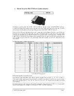
  20-pin 1.27mm Cortex Debug Cable Adapter 


Ordering code 

IC50113 


Note: This product is obsolete and is fully replaced with IC50118 

IC50113 Cortex-M Adapter Board is used to connect the iC5000 development system to Cortex-M based target. 
It  connects  to  Debug/Trace  module  on  one  side  and  to  the  target  debug  connector  on  the  other  side.  It  can  be 
used for targets featuring 20-pin 1.27mm pitch target debug connector with Cortex-M pinout. 

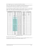
The following pinout is valid on the target side:  

Signal 

direction 

Signal description  Signal  Pin 

Pin 

Signal 

Signal description 

Signal 

direction 

Reference voltage  VTref 

SWDIO/TMS 

SWD/JTAG 

I/O 


Ground 

GND 

SWCLK/TCK 

SWD/JTAG 


Ground 

GND 

SWO/TDO 

SWD/JTAG 


Ground 

GND 

NC/TDI 

SWD/JTAG 


Ground 

GND 

10 

nSRST 

System Reset 

I/O 


Ground 

GND 

11 

12 

TRCLK 

Trace Clock 


Ground 

GND 

13 

14 

TRD0 

Trace Data 0 


Ground 

GND 

15 

16 

TRD1 

Trace Data 1 


Ground 

GND 

17 

18 

TRD2 

Trace Data 2 


Ground 

GND 

19 

20 

TRD3 

Trace Data 3 

20-pin Cortex-M pinout 

Note:  20-pin  1.27mm  Cortex-M  Cable  Adapter  features  resettable  fuses  on  pins  1,  2,  4,  6,  8  and  10.  These 
protect debug signals against overcurrent and cycle back to a conductive state after the excessive current  fades 
away. Signals on pins 12, 14, 16, 18 and 20 are protected via 100 ohm serial resistors. 

The adapter connects to the target via a 20-pin 1.27mm connector (for example SAMTEC: FFSD-10-01-N). A 
target should feature a matching part (for example SAMTEC: FTSH-110-01-F-DV-K). 


Summary of Contents for iC5000

Page 1: ...e our alternative products iSystem constantly yields for development and therefore certain pictures in this documentation may vary slightly from the actual product you received The differences should be minor but should you find more serious inconsistencies of the product with the documentation please contact your local distributor for more information This document and all documents accompanying ...

Page 2: ...iC5000 Base Unit features 256MB of analyzer storage buffer There are three status LEDs on the iC5000 Base Unit The status LEDs inform the user of the current status of the emulation system Their meaning is When lit the unit is turned on R When lit the target application being controlled is running F When lit the unit is free for communication i e winIDEA can connect to it Ordering code IC50000 or ...

Page 3: ...Debug Trace Module and cable adapter without I O module The necessary power supply IC30000 PS is delivered beside the iC5000 unit IC30000 PS An optional 12V power supply for Car cigarette lighter plug can be ordered under the IC30000 PS CAR12V ordering code IC30000 PS CAR12V Note Use only original iSYSTEM accessories for powering the iC5000 If you wish to use a power supply different from the deli...

Page 4: ... license is required to debug the target based on a specific architecture Valid input voltage range for all debug signals is between 1 8 5 5V Note Typically IC50000 and IC50020 modules already come assembled together when delivered to the user The user only needs to connect a specific cable adapter via 40 pin flat cable through which the development system then connects to the target iC5000 develo...

Page 5: ...should be facing away from the iC5000 Base Unit with the red edge wire on the side of the DTM 1 marking Align the orientation key notch of the cable connector with the notch on the iC5000 40 pin connector marked with 1 Press the cable connector carefully straight down until the latches lock Do not press only on one side of the connector as this can in worst case bend the corner pins of the DTM 1 c...

Page 6: ...t cables Be gentle when connecting one connector to the other Do not use any excessive force observe the orientation key and connector notches First connect the 30 pin flat cable to the iC5000 DTM 2 connector The cable should be facing away from the iC5000 Base Unit with the red edge wire on the side of the DTM 2 marking Align the orientation key notch of the cable connector with the notch on the ...

Page 7: ...cy long duration trace analyzer session measurements All digital signals are 3 3V LVTTL compatible and are ESD protected All analog signals have a Schottky diode over undervoltage protection except the Current Sense signals The maximum voltage on the Current Sense probe is 60V Nominal sampling rate is 1MSPS Connectors iC5000 I O Module Connectors Pinout 10 pin header for the System Port 16 pin hea...

Page 8: ...troduced by power supply target emulator which does not have the power outlet ground connected with the power supply ground power outlets which have different ground potentials PC when iC5000 connects to the PC through the USB port Connecting a dedicated grounding wire which is shipped with the iC5000 unit between the iC5000 system and the target before the target debug cable adapter is connected ...

Page 9: ...functionality is required iSYSTEM development tools feature a hardware based license scheme which saves costs comparing to per seat based licenses All licenses are kept in the iC5000 development system which conveniently allows moving iC5000 unit from one development seat to another When new iC5000 system is shipped from iSYSTEM CPU architecture and trace licenses are preprogrammed by the iSYSTEM ...

Page 10: ... select when the Emulator is attached to the PC s USB port The Emulator is selected in the Device pull down menu When the Emulator is connected to the USB port of a computer for the first time Windows will detect a new device and may prompt you for the driver for it Specify the path to the USB directory in the winIDEA installation directory If only one emulator is connected to the PC via the USB t...

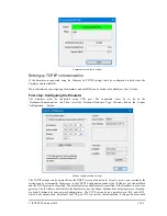
Page 11: ...k on the System Configuration button System configuration options The TCP IP settings can be obtained from the DHCP server on the network If such a server is not available the settings can be set manually In this case in the TCP IP Configuration window the IP Address the Subnet Mask and the TCP Port must be specified The default gateway address must be specified if the Emulator is used via a gatew...

Page 12: ...ll also find device serial number as it is shown on the next picture Second step Configuring communication There are two ways of configuring TCP IP in winIDEA manually or by automatic discovery Manual Configuration Select the Hardware Communication tab Hardware Communication tab Select the TCP IP button and enter the IP Address and the TCP Port as entered above into the Emulator Connect the Emulat...

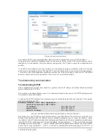
Page 13: ...address or the TCP Port First make sure the Subnet Mask is correct The subnet mask should be the same in the TCP IP configuration of your computer and in the Emulator To find out the TCP IP settings of your computer open the command prompt and type ipconfig The computer will return something like this Ethernet adapter Local Area Connection Connection specific DNS Suffix IP Address 210 121 92 121 S...

Page 14: ...it up in the Emulator and in winIDEA and try again When the ping is not more required stop it using the keyboard shortcut Control C If more Emulators are connected to the Ethernet and have the same IP set only one will be active Every Emulator must have a unique IP Troubleshooting the USB During winIDEA installation USB driver is also installed Very rarely after you power on the emulator which you...

Page 15: ...CB design or a combination of both IC5000 has the ability to compensate for these issues via Trace Line Calibration functionality which allows shifting threshold voltage and clock phase at the capture time of the trace data When Trace Line Calibration is performed it auto scans over these two dimensions and searches for valid and invalid settings and finds an optimum data eye Example Let s assume ...

Page 16: ...wer frequency with large Data eyes Trace Line Calibration window scan has been performed and applied X invalid area valid area R recommended o currently used Higher frequency Valid Data eyes shown on upper data signal and how the clock lower must be delayed ...

Page 17: ...iver characteristics Trace clock should be clean of crosstalk if possible with double distance to closest nets Trace clock should have only point to point connection any stubs should be avoided It is strongly recommended also for other data lines to be point to point only If any stubs are needed they should be as short as possible when longer are required there should be a possibility to optionall...

Page 18: ...trace data will be missing It doesn t mean any hardware failure Possible solutions lower the target CPU clock increase Nexus clock divider which yields lower Nexus clock but at the same time Nexus is more prone to overflows then changing the trace port width e g from 16 bit to 12 bit or from 12 bit to 4 bit reduces the Nexus information bandwidth Note that possible port size varies depending on th...

Page 19: ...0155 Mictor 38 pin PPC4xx RISCTrace Cable Adapter IC50156 50 pin Samtec MPC5xxx Nexus 16 bit Cable Adapter IC50158 Mictor 38 pin MPC5xx Nexus 8 bit Cable Adapter IC50160 16 pin 2 54mm Infineon JTAG Cable Adapter IC50160 ECU14 10 pin 1 27mm Tricore ECU14 Cable Adapter IC50160 MEDC17 10 pin 1 27mm Tricore MEDC17 Cable Adapter IC50162 6 pin 2 54mm Infineon I2C Cable Adapter IC50163 10 pin 1 27mm Infi...

Page 20: ...Pin Pin Signal Signal description Signal direction I Reference voltage VTref 1 2 SWDIO TMS SWD JTAG I O Ground GND 3 4 SWCLK TCK SWD JTAG O Ground GND 5 6 SWO TDO SWD JTAG I Ground GND 7 8 NC TDI SWD JTAG O Ground GND 9 10 nSRST System Reset I O Ground GND 11 12 TRCLK Trace Clock I Ground GND 13 14 TRD0 Trace Data 0 I Ground GND 15 16 TRD1 Trace Data 1 I Ground GND 17 18 TRD2 Trace Data 2 I Ground...

Page 21: ...n Signal Pin Pin Signal Signal description Signal direction I Reference voltage VTref 1 2 NC Not Connected O JTAG nTRST 3 4 GND Ground O SWD JTAG NC TDI 5 6 GND Ground I O O SWD JTAG SWDIO TMS 7 8 GND Ground O SWD JTAG SWDCLK TCK 9 10 GND Ground I Return TCK RTCK 11 12 GND Ground I SWD JTAG SWO TDO 13 14 GND Ground I O System Reset nSRST 15 16 GND Ground O Debug request DBGRQ 17 18 GND Ground I De...

Page 22: ...t side Signal direction Signal description Signal Pin Pin Signal Signal description Signal direction Output Standard JTAG TMS 1 2 nTRST Standard JTAG Output Output Standard JTAG TDI 3 4 GND Ground Input Reference voltage VTref 5 6 NC Not connected Input Standard JTAG TDO 7 8 GND Ground Input Return TCK RTCK 9 10 GND Ground Output Standard JTAG TCK 11 12 GND Ground Input Debug Acknowledge BERR 13 1...

Page 23: ...n Signal Signal description Signal direction Not Connected NC 1 2 GND Ground O Debug JTAG nTRST 3 4 GND Ground O Debug JTAG TDI 5 6 GND Ground O Debug JTAG TMS 7 8 GND Ground O Debug JTAG TCK 9 10 GND Ground I Debug JTAG TDO 11 12 nSRST System Reset I O I Reference voltage VTref 13 14 GND Ground 14 pin ARM pinout Note 14 pin 2 54mm ARM Cable Adapter features resettable fuses on all pins These fuse...

Page 24: ...O TMS SWD JTAG I O Ground GND 3 4 SWCLK TCK SWD JTAG O Ground GND 5 6 SWO TDO SWD JTAG I Ground GND 7 8 NC TDI SWD JTAG O Ground GND 9 10 nSRST System Reset I O Ground GND 11 12 TRCLK Trace Clock I Ground GND 13 14 TRD0 Trace Data 0 I Ground GND 15 16 TRD1 Trace Data 1 I Ground GND 17 18 TRD2 Trace Data 2 I Ground GND 19 20 TRD3 Trace Data 3 I 20 pin Cortex M pinout Note 20 pin 1 27mm Cortex M Cab...

Page 25: ... 6 SWO TDO SWD JTAG I Ground GND 7 8 NC TDI SWD JTAG O Ground GND 9 10 nSRST System Reset I O Ground GND 11 12 TRCLK Trace Clock I Ground GND 13 14 TRD0 Trace Data 0 I Ground GND 15 16 TRD1 Trace Data 1 I Ground GND 17 18 TRD2 Trace Data 2 I Ground GND 19 20 TRD3 Trace Data 3 I 20 pin Cortex M pinout Blue colored signals are required for trace Note 20 pin 1 27mm AMPMODU Cortex M Cable Adapter feat...

Page 26: ... ARM ETM 16 bit cable adapter The following pinout is valid on the target side Signal direction Signal Pin Pin Signal Signal direction NC 1 2 NC NC 3 4 NC NC 5 6 TRACECLK I NC 7 8 NC I O nSRST 9 10 NC I TDO 11 12 VTref I NC 13 14 NC O TCK 15 16 TRACEPKT 7 I O TMS 17 18 TRACEPKT 6 I O TDI 19 20 TRACEPKT 5 I O nTRST 21 22 TRACEPKT 4 I NC 23 24 TRACEPKT 3 I NC 25 26 TRACEPKT 2 I NC 27 28 TRACEPKT 1 I...

Page 27: ...3 pinout The following pinout is valid on the target side Signal direction Signal Pin Pin Signal Signal direction NC 1 2 NC NC 3 4 NC NC 5 6 TRACECLK I NC 7 8 NC I O nSRST 9 10 NC I TDO 11 12 VTref I NC 13 14 NC O TCK 15 16 TRACEPKT 7 I O TMS 17 18 TRACEPKT 6 I O TDI 19 20 TRACEPKT 5 I O nTRST 21 22 TRACEPKT 4 I I TRACEPKT 15 23 24 TRACEPKT 3 I I TRACEPKT 14 25 26 TRACEPKT 2 I I TRACEPKT 13 27 28 ...

Page 28: ... excessive current fades away Signals on pins 6 16 18 20 and 22 38 are protected via 47 ohm serial resistors The adapter connects to the target via a 38 pin Mictor connector Tyco Electronics 5767055 1 A target should feature a matching part for example Tyco Electronics 5767081 1 in SMT technology Texas Instruments TMS570 Microcontrollers Targets based on Texas Instruments TI ARM microcontroller ca...

Page 29: ...lowing pinout is valid on the target side Signal direction Signal Pin Pin Signal Signal direction I VTref 1 2 TMS O O TCK 3 4 TDO I O TDI 5 6 nSRST I O O RTCK 7 8 nTRST_PD O O nTRST_PU 9 10 NC NC 11 12 NC I TRACECLK 13 14 NC NC 15 16 GND I TRACECTL 17 18 NC I TRACEDATA0 19 20 NC I TRACEDATA1 21 22 NC I TRACEDATA2 23 24 NC I TRACEDATA3 25 26 NC I TRACEDATA4 27 28 NC I TRACEDATA5 29 30 NC I TRACEDAT...

Page 30: ...on Signal Pin Pin Signal Signal description Signal direction I Reference voltage VTref 1 2 SWDIO TMS SWD JTAG I O Ground GND 3 4 SWCLK TCK SWD JTAG O Ground GND 5 6 SWO TDO SWD JTAG I Ground GND 7 8 NC TDI SWD JTAG O Ground GND 9 10 nSRST System Reset I O 10 pin Cortex M pinout Note 10 pin 1 27mm Cortex M Cable Adapter features resettable fuses on pins 1 2 4 6 8 and 10 These fuses protect debug si...

Page 31: ... Ground GND 5 6 SWO TDO SWD JTAG I Ground GND 7 8 NC TDI SWD JTAG O Ground GND 9 10 nSRST System Reset I O NC_CAPGND 11 12 TRCLK Trace Clock I NC_CAPGND 13 14 TRD0 Trace Data 0 I Ground GND 15 16 TRD1 Trace Data 1 I Ground GND 17 18 TRD2 Trace Data 2 I Ground GND 19 20 TRD3 Trace Data 3 I 20 pin Cortex M pinout Blue colored signals are required for trace Note 20 pin 1 27mm Cortex M Cable Adapter f...

Page 32: ... Standard JTAG TCK 11 12 GND Ground I Emulation pins EMU0 13 14 EMU1 Emulation pins I I O System Reset nSRST 15 16 GND Ground I Emulation pins EMU2 17 18 EMU3 Emulation pins I I Emulation pins EMU4 19 20 GND Ground 20 pin Compact TI 20 pinout Jumpers J1 and J2 Jumpers J1 and J2 selects whether EMU0 J1 or EMU1 J2 is tied to pull up position 1 2 or directly to the GND position 2 3 EMU signals functi...

Page 33: ...0 DSO I GND 11 12 PSTDDATA7 I I PSTDDATA6 13 14 PSTDDATA5 I I PSTDDATA4 15 16 PSTDDATA3 I I PSTDDATA2 17 18 PSTDDATA1 I I PSTDDATA0 19 20 GND Motorola Reserved 21 22 Motorola Reserved GND 23 24 PSTCLK I NC 25 26 TEA O ColdFire 26 pin target pinout Blue colored signals are required for trace Note 26 pin 2 54 mm ColdFire Cable Adapter features resettable fuses on pins 2 4 7 8 9 10 24 and 26 These pr...

Page 34: ... valid on the target side Signal direction Signal description Signal Pin Pin Signal Signal description Signal direction I O BGND BGND 1 2 GND Ground Not connected NC 3 4 RESET System Reset I O Not connected NC 5 6 VTref Reference voltage I 6 pin BDM pinout Note 6 pin BDM Cable Adapter features resettable fuses on pins 1 2 4 and 6 These fuses protect debug signals against overcurrent and cycle back...

Page 35: ...ignal description Signal Pin Pin Signal Signal description Signal direction I O BGND BGND 1 2 GND Ground I data out PDO 3 4 RESET System Reset I O I clock PDOCLK 5 6 VTref Reference voltage I 6 pin BDM pinout Note 6 pin BDM Cable Adapter features resettable fuses on pins 1 2 4 and 6 These fuses protect debug signals against overcurrent and cycle back to a conductive state after the excessive curre...

Page 36: ...te machine Because JTAG TAP state machine can be reset also by TMS and TCK this pin is optional also for the debugger If microcontroller has JCOMP pin but it is not connected to the target debug connector then it must be set to non active state in the target via a pull up resistor If not then JTAG TAP state machine remains in reset and debugging is not possible 14 pin 2 54mm MPC5xxx Cable Adapter ...

Page 37: ...Refer to iSYSTEM Freescale MPC5xxx ST SPC56 Family On Chip Emulation technical notes document for more details on the Force periodic Nexus SYNC option use Note that the EVTI Nexus Event In CPU pin may be shared with other CPU functionalities For instance on MPC5516 the same pin can operate as GPIO EBI read write or EVTI Whenever the CPU pin is configured and used for EVTI alternate operation J2 mu...

Page 38: ...ble adapter Jumper J2 EVTIN Under some circumstances it can happen that the debugger cannot find any absolute program counter message in the analyzed Nexus trace block Consequentially trace reconstruction fails and errors or nothing gets displayed in the trace window To avoid such situations the debugger can feed periodic signal to the EVTIN CPU pin connecting to the on chip Nexus engine which the...

Page 39: ... 38 MSEO0 I MPC5xxx and SPC56 16 bit Nexus target pinout Blue colored signals are required for trace Note Mictor 38 pin MPC5xxx Nexus 8 bit Cable Adapter features resettable fuses on pins 9 10 11 12 15 17 19 and 21 These protect debug signals against overcurrent and cycle back to a conductive state after the excessive current fades away Signals on pins 16 18 20 22 24 26 28 30 32 34 36 and 38 are p...

Page 40: ...e reconstruction fails and errors or nothing gets displayed in the trace window To avoid such situations the debugger can feed periodic signal to the EVTIN CPU pin connecting to the on chip Nexus engine which then periodically generates and broadcasts program counter synchronization messages In order to use this feature jumper J2 must be bridged and the Force periodic Nexus SYNC option in the Hard...

Page 41: ...ia 47 ohm serial resistors The adapter connects to the target via a 38 pin Mictor connector Tyco Electronics 5767055 1 A target should feature a matching part for example Tyco Electronics 5767081 1 in the SMT technology Ordering code IAMIC38SAM50MPC IAMIC38SAM50MPC adapter Some targets based on Freescale Qorivva Power Architecture or PX Series Power Architecture microcontroller s e g MPC5675K can ...

Page 42: ...MDO4 21 22 NC GND 23 24 GND I MDO5 25 26 NC I MDO6 27 28 NC GND 29 30 GND I MDO7 31 32 NC I MDO8 33 34 NC GND 35 36 GND I MDO9 37 38 NC I MDO10 39 40 NC GND 41 42 GND I MDO11 43 44 MDO13 I I MDO12 45 46 MDO14 I GND 47 48 GND I MDO15 49 50 NC 50 pin Samtec ERF8 Nexus target connector pinout Blue colored signals are required for trace The adapter connects to the target via a 50 pin ERM8 connector fo...

Page 43: ...hm pull down O O Standard JTAG TDI 3 4 TRST Standard JTAG O I Status optional HALTED 5 6 VTref Reference voltage I O Standard JTAG TCK 7 8 CKSTP_IN Status optional O O Standard JTAG TMS 9 10 NC Not Connected O Soft Reset SRESET 11 12 GND Ground O Hard Reset HRESET 13 14 NC Not Connected I Status optional CKSTP_OUT 15 16 GND Ground 16 pin Freescale COP target pinout Note 16 pin 2 54mm Freescale COP...

Page 44: ...or instead of the popular 38 pin Mictor target debug connector The following pinout is valid on the target side Signal direction Signal Pin Pin Signal Signal direction NC 1 2 NC NC 3 4 NC I TDO 5 6 RDY O RESET 7 8 VTREF I O EVTIN 9 10 GND O TRST 11 12 GND O TMS 13 14 GND O TDI 15 16 GND O SWCLK TCK 17 18 GND I MDO0 19 20 GND I MCKO 21 22 GND I EVTO 23 24 GND I MSEO0 25 26 MDO9 I I MDO1 27 28 GND I...

Page 45: ...ent and cycle back to a conductive state after the excessive current fades away Signals on pins 19 21 23 25 26 27 29 31 35 37 39 41 43 45 47 49 and GND are protected via 47 ohm serial resistors The adapter connects to the target via a 51 pin GLENAIR connector for example GLENAIR M83513 02 GN A target should feature a matching part for example GLENAIR M83513 01 GN ...

Page 46: ...TCK 15 16 NC O TMS 17 18 NC O TDI 19 20 NC O NTRST 21 22 NC NC 23 24 NC I BS0 25 26 TS0 I I BS1 27 28 TS1 I I BS2 29 30 TS2 I I BS3 31 32 TS3 I I BS4 33 34 TS4 I I BS5 35 36 TS5 I I BS6 37 38 TS6 I PPC4xx RISCTrace target pinout Blue colored signals are required for trace Note Mictor 38 pin MPC5xxx Nexus 16 bit Cable Adapter features resettable fuses on pins 7 9 11 12 15 17 19 and 21 These protect...

Page 47: ...ace reconstruction fails and errors or nothing gets displayed in the trace window To avoid such situations the debugger can feed periodic signal to the EVTIN CPU pin connecting to the on chip Nexus engine which then periodically generates and broadcasts program counter synchronization messages In order to use this feature jumper J2 must be bridged and the Force periodic Nexus SYNC option in the Ha...

Page 48: ...GND 41 42 GND I MDO11 43 44 MDO13 I I MDO12 45 46 MDO14 I GND 47 48 GND I MDO15 49 50 NC MPC5xxx and SPC56 50 pin 16 bit Nexus target pinout Blue colored signals are required for trace Note 50 pin Samtec MPC5xxx Nexus 16 bit Cable Adapter features resettable fuses on pins 2 4 6 8 10 12 16 and 20 These protect debug signals against overcurrent and cycle back to a conductive state after the excessiv...

Page 49: ... 15 16 Reserved O MSEI 17 18 Reserved O MDI0 19 20 Reserved O RSTI 21 22 Reserved I MDO0 23 24 Reserved I MDO1 25 26 Reserved I MDO2 27 28 Reserved I MDO3 29 30 Reserved I MDO4 31 32 Reserved I MDO5 33 34 Reserved I MDO6 35 36 Reserved I MDO7 37 38 MSEO I MPC5xx 8 bit Nexus target pinout Blue colored signals are required for trace Note Mictor 38 pin MPC5xx Nexus 16 bit Cable Adapter features reset...

Page 50: ...SEI 13 14 NC O MDI0 15 16 NC O MCKI 17 18 GND MDO0 19 20 GND I MCKO 21 22 GND I EVTO 23 24 GND I MSEO 25 26 VENDOR_IO1 I O I MDO1 27 28 GND I MDO2 29 30 GND I MDO3 31 32 GND O MDI1 33 34 GND NC 35 36 GND I MDO4 37 38 GND I MDO5 39 40 GND I MDO6 41 42 GND I MDO7 43 44 GND NC 45 46 GND NC 47 48 GND I O VENDOR_IO2 49 50 GND Nexus 50 pin AMPMODU System 50 target connector Blue colored signals are requ...

Page 51: ...d JTAG TDO 3 4 GND Ground O optional CPUCLK 5 6 GND Ground O Standard JTAG TDI 7 8 RESET Power On Reset O O Standard JTAG TRST 9 10 BRK_OUT Break Output I I Standard JTAG TCLK 11 12 GND Ground O Break Input BRK_IN 13 14 OCDS_E optional O Not Connected NC 15 16 NC Not Connected 16 pin Infineon JTAG target pinout Mandatory pins on the microcontroller side are TMS TDO TDI TRST TCLK and RESET BRK_IN a...

Page 52: ...in Signal Signal description Signal direction O Break Input BRK_IN 1 2 TRST Standard JTAG O Ground GND 3 4 TCLK Standard JTAG O O Standard JTAG TMS 5 6 BRK_OUT Break Output I O Power On Reset RESET 7 8 TDI Standard JTAG O I Reference voltage VTref 9 10 TDO Standard JTAG I 10 pin Bosch MEDC17 target pinout Mandatory pins on the microcontroller side are TMS TDO TDI TRST TCLK and RESET BRK_IN and BRK...

Page 53: ...gnal can be used optionally Note 10 pin 1 27mm TriCore ECU14 Cable Adapter features resettable fuses on all connected pins These protect debug signals against overcurrent and cycle back to a conductive state after the excessive current fades away Jumper J1 Jumper J1 has been put on the adapter only for making provision for future extensions of the ECU14 target connection The USERIO signal target d...

Page 54: ...2 3 Hot Attach operation is configured In this case all debug signals from the iC5000 unit are disconnected and the target starts running as soon as the power is applied to the target When Hot Attach command is issued from winIDEA the debugger connects to the MCU and control over the MCU is taken without resetting the MCU Depending on the target MCU refer to the XC166 XC2000 or the TriCore technic...

Page 55: ... emulator and programming mode selected During the debug download first user flash is erased then the application code programmed into the flash and at the end the complete flash is read back This last step is required since the code memory can be no longer read once the MCU is in the debug mode Beside of the user flash SP41 has also Firmware ROM which cannot be read by the debugger After the debu...

Page 56: ...soon as the power is applied to the target When Hot Attach command is issued from winIDEA the debugger connects to the MCU and control over the MCU is taken without resetting the MCU Depending on the target MCU refer to the XC166 XC2000 or the TriCore technical notes document for more details on Hot Attach configuration and use The following pinout is valid on the target side Signal direction Sign...

Page 57: ...nd is issued from winIDEA the debugger connects to the MCU and control over the MCU is taken without resetting the MCU Depending on the target MCU refer to the TriCore technical notes document for more details on Hot Attach configuration and use The following pinout is valid on the target side Signal direction Signal Pin Pin Signal Signal direction Not Connected 1 2 Vref I Not Connected 3 4 DAP0 O...

Page 58: ... Connected NC 13 14 FLMD0 Flash Mode O I Reset In RESET IN 15 16 TOOL1 CLK Clock Input I 16 pin Renesas 78K0R Serial Debug target pinout If the Supply 5V to the target option is checked in the Hardware Emulation Options CPU Setup Advanced tab the debugger supplies 5V at Vcc pin pin 4 of the target debug connector which can be used to power the target Maximum target current consumption should not e...

Page 59: ...AG O Ground GND 5 6 TDI Debug JTAG O Ground GND 7 8 TRST Debug JTAG O Ground GND 9 10 NC Not Connected Ground GND 11 12 RESET CPU Reset I O Ground GND 13 14 FLMD0 Flash Mode O Ground GND 15 16 RDY Synchronization I Ground GND 17 18 TDO Debug JTAG I Ground GND 19 20 VDD Reference voltage I 20 pin Renesas V850 RH850 target pinout Note 20 pin 2 54mm V850 RH850 Cable Adapter features resettable fuses ...

Page 60: ... Reserved Ground GND B4 A4 Reserved Reserved Ground GND B5 A5 Reserved Reserved Ground GND B6 A6 Reserved Reserved Ground GND B7 A7 DDI N Wire O Ground GND B8 A8 DCK N Wire O Ground GND B9 A9 DMS N Wire O Ground GND B10 A10 DDO N Wire I Reserved Reserved B11 A11 DRST N Wire O Reserved Reserved B12 A12 RESET Reset O I Reference Voltage VTRef B13 A13 FLMD0 Flash Mode O 26 pin Renesas V850 target pin...

Page 61: ...ted O Debug JTAG NTRST 3 4 ASEMD Status read I I Debug JTAG TDO 5 6 GND Ground O Mode select ASEBRK 7 8 VTREF Reference voltage O O Debug JTAG TMS 9 10 GND Ground O Debug JTAG TDI 11 12 GND Ground RESET IN RESET 13 14 GND_DETECT Ground detect I 14 pin SuperH target pinout Note 14 pin 2 54mm SuperH cable adapter features resettable fuses on all pins except for pin 14 where serial resistor of 100ohm...

Page 62: ...d in the Hardware Emulation Options CPU Setup Advanced tab the debugger supplies 5V at 5V OUT pin pin 10 of the target debug connector which can be used to power the target Maximum target current consumption should not exceed 50mA Note 10 pin Renesas 78K0R Serial Debug Cable Adapter features resettable fuses on all connected pins These protect debug signals against overcurrent and cycle back to a ...

Page 63: ...d NC 5 6 NC Not Connected Not Connected NC 7 8 NC Not Connected O Communication line X1 9 10 NC Not Connected Not Connected NC 11 12 NC Not Connected I O Communication line X2 13 14 FLMD0 Flash Mode O I Reset In RESET IN 15 16 NC Not Connected 16 pin Renesas 78K0 Serial Debug target pinout The adapter connects to the target via a 10 pin 2 54 mm connector for example Yamaichi FAS 1001 2101 2 OBF A ...

Page 64: ...ound O Reset Out RESET_OUT 13 14 GND Ground 14 pin Renesas RL78 Serial Debug target pinout If the Supply 5V to the target option is checked in the Hardware Emulation Options CPU Setup Advanced tab the debugger supplies 5V at VDD pin pin 8 of the target debug connector which can be used to power the target Maximum target current consumption should not exceed 50mA Some RL78 devices may have two powe...

Page 65: ... Ground O Debug JTAG TRST 3 4 FLMD0 Flash Mode O I Debug JTAG TDO 5 6 FLMD1 Flash Mode O O Debug JTAG TDI 7 8 VTREF Reference voltage I O Debug JTAG TMS 9 10 NC Not Connected I Synchronization RDY 11 12 GND Ground I O CPU Reset RESET 13 14 GND Ground 14 pin Renesas RH850 target pinout Note 14 pin 2 54mm RH850 Cable Adapter features resettable fuses on all pins except for pin 11 These fuses protect...

Page 66: ...ection Signal Pin Pin Signal Signal direction I JP05 RDY 1 2 RESET I O O JP02 TCK 3 4 JP00 TDI O O JP03 TMS 5 6 JP04 TRST O I JP01 TDO 7 8 FLMD0 O 3V3 9 10 GND 10 pin Renesas RH850 proprietary EPS target pinout Note 10 pin 1 27mm RH850 Cable Adapter features resettable fuses on all pins except for pin 1 and pin 10 These fuses protect debug signals against overcurrent and cycle back to a conductive...

Page 67: ...ection I MDO12 1 2 MDO13 I I MDO14 3 4 MDO15 I I MDO9 5 6 NC NC 7 8 MDO8 I O NRESET 9 10 EVTI O I TDO 11 12 VTREF I I MDO10 13 14 RDY I O TCK 15 16 MDO7 I O TMS 17 18 MDO6 I O TDI 19 20 MDO5 I O TRST 21 22 MDO4 I I MDO11 23 24 MDO3 I NC 25 26 MDO2 I NC 27 28 MDO1 I NC 29 30 MDO0 I NC 31 32 EVTO I NC 33 34 MCKO I NC 35 36 MSEO1 I O FLMD0 37 38 MSEO0 I Mictor 38 pin Renesas RH850 F1H 16 bit Nexus ta...

Page 68: ...n the target side Pin Signal Signal description Signal direction 1 VDD Reference voltage I 2 SWIO Debug SWIM pin I O 3 GND Ground 4 RST Reset O 4 pin ERNI ST STM8 target pinout Note 4 pin ERNI ST STM8 Cable Adapter features resettable fuses on all pins These fuses protect debug signals against overcurrent and cycle back to a conductive state after the excessive current fades away The adapter ends ...

Page 69: ...gging including some troubleshooting tips Operating Environment Operating temperature between 10 C and 40 C Humidity 5 to 80 RH Storage temperature between 10 C and 60 C Dimensions 127 x 127x 54 mm Note Consult with iSYSTEM when using equipment outside of these parameters Disclaimer iSYSTEM assumes no responsibility for any errors which may appear in this document reserves the right to change devi...

Reviews: