background image

User Guide 083

UG083.0

July 25, 2016

Submit Document Feedback

4

Software Installation Guide

The ISL76534EVAL1Z software can be installed from an installer 
file downloaded from the 

ISL76534

 product information page on 

the Intersil web site.

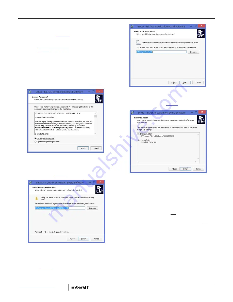
Launch the “

isl76534_installer.exe

” file and follow the 

instructions (

Figure 5

). The default installation adds an “Intersil” 

directory to the “Start Menu\Programs” tree. That directory will 
contain a shortcut to the ISL76534 executable, and an 
uninstaller. 

The default install option places the main program files in the 
C:\Program Files\Intersil\ISL76534 directory; however, the 
location can be customized, if desired.

Click Next to continue to the license agreement (

Figure 5

).

Read the license agreement, choose to accept (or not accept) the 
license agreement, then click Next. The Select Destination 
Location window opens (

Figure 6

). 

To use a directory different from the default location, click the 
Browse button. Click Next to continue to the Select Start Menu 
Folder screen (

Figure 7

).

Click Next to create the Intersil folder in the Start menu. The 
Ready to Install window opens (

Figure 8

).

Click Install to copy all the necessary files to the PC. Installation 
is now complete. Reboot the PC if requested.

Hardware Set-up Guide

Initial Board Jumper Positioning 

JP1 - Is used to set the logic level of the Write Protection pin WP. 
Shorting JP1-1 and -2 grounds the WP and prevents I

2

C data 

write to the internal DAC registers. This is the default if the pin is 
left floating. Shorting JP1-2 and -3 provides a high on the WP and 
thereby allows a data write to the internal DAC registers. Note the 
pin has an internal pull down to GND.

JP2 - This pin determines the 7-bit I

2

C device address. Shorting 

JP1-1 and -2 grounds the A0 and sets it to low which equates to a 
device address of 0x74. This is the default setting if the pin is left 
floating. Shorting JP1-2 and -3 provides a high on the A0, which 
sets the I

2

C address to 0x75 (pulled up externally). Note that the 

pin has an internal pull down to GND.

After the software is installed, the evaluation board is ready to be 
interfaced through the PC.

FIGURE 5. LICENSE AGREEMENT


FIGURE 6. SELECT DESTINATION LOCATION


FIGURE 7. SELECT START MENU FOLDER


FIGURE 8. BEGIN INSTALLATION


Summary of Contents for ISL76534EVAL1Z

Page 1: ...nel reference voltage outputs I2C programmable 14 channel gamma references 10 bit resolution with buffered outputs 1 channel VCOM calibrator with 10 bit resolution High output current VCOM amplifier U...

Page 2: ...R SUPPLY REFIN RAM 14x10 CONTROL BYTE EEPROM VCOM DAC 10 GND DAC15 GND REFIN WP WP ACTIVE LOW OUT1 OUT2 VCOM AMPLIFIER DAC1 10 10 DAC2 OUT3 10 DAC3 OUT4 OUT5 DAC4 10 10 DAC5 OUT6 10 DAC6 OUT7 OUT8 DAC...

Page 3: ...nd how to use the Windows interface to read and write to the ISL76534 data register and EEPROM Evaluation Software The next section explains how to install the Graphical User Interface GUI software wh...

Page 4: ...ext to create the Intersil folder in the Start menu The Ready to Install window opens Figure 8 Click Install to copy all the necessary files to the PC Installation is now complete Reboot the PC if req...

Page 5: ...ay appear displaying the status of the USB module hardware If a Found New Hardware window appears asking for the location of device drivers please contact Intersil for a new USB module Using the Softw...

Page 6: ...ng the PC verify that the following files are in the following locations ISL76534 exe in C Program Files Intersil ISL76534 isilhid dll in C Program Files Intersil ISL76534 If the dialog shown in Figur...

Page 7: ...the thermal pad is not connected to GND then it should be electrically isolated Maximize use of AC decoupled PCB layers All signal I O lines should be routed over continuous ground planes i e no spli...

Page 8: ...User Guide 083 8 UG083 0 July 25 2016 Submit Document Feedback Schematic FIGURE 13 SCHEMATIC...

Page 9: ...User Guide 083 9 UG083 0 July 25 2016 Submit Document Feedback FIGURE 14 SCHEMATIC Continued Schematic Continued...

Page 10: ...GENERIC H1045 00104 50V10 31 ea C1 C2 C6 C12 C39 Do Not Populate Multilayer Cap GENERIC H1045 OPEN 34 ea R1 R5 R7 R15 R21 R31 R37 R46 R51 R58 Do Not Populate Metal Film Chip Resistor GENERIC H2505 DN...

Page 11: ...User Guide 083 UG083 0 July 25 2016 Submit Document Feedback 11 PCB Layouts FIGURE 15 SILK LAYER TOP FIGURE 16 TOP LAYER COMPONENT SIDE...

Page 12: ...User Guide 083 UG083 0 July 25 2016 Submit Document Feedback 12 FIGURE 17 INTERNAL LAYER 2 FIGURE 18 INTERNAL LAYER 3 PCB Layouts Continued...

Page 13: ...User Guide 083 UG083 0 July 25 2016 Submit Document Feedback 13 FIGURE 19 BOTTOM LAYER SOLDER SIDE FIGURE 20 SILKSCREEN BOTTOM PCB Layouts Continued...

Page 14: ...0 8 1 2 0 128 256 384 512 640 768 896 1024 DAC CODE DEC LINEARITY LSB TYPICAL PRODUCTION UNIT AVDD REFIN 15V DVDD 3 3V NO LOAD 0 10 0 08 0 06 0 04 0 02 0 00 0 02 0 04 0 06 0 08 0 10 0 128 256 384 512...

Reviews: