TC1796
Peripheral Units (Vol. 2 of 2)
General Purpose Timer Array (GPTA)
User’s Manual
24-6
V2.0, 2007-07
GPTA, V2.0
24.2
GPTA0/GPTA1 Kernel Description
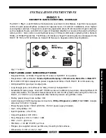
The functionality of the General Purpose Timer Arrays GPTA0/GPTA1 kernel is
described in this section. Clock control, address decoding, and service (interrupt)
request control are managed outside the GPTA0/GPTA1 module kernel.
shows a global block diagram of the GPTA module kernel.
Figure 24-2 Block Diagram of GPTA Kernel
Each GPTA0/1 kernel has 56 input signals, 112 output signals, and four input signals,
that can be connected to port pins or other on-chip logic units (see
Implementation” on Page 24-247
for the TC1796 specific interconnections). Further,
several clock input and output signals are provided.
Interrupt
Control
MCB05911
Clock
Control
Address
Decoder
f
GPTA
SR[37:00]
GPTA Module Kernel
Clock Generation Unit
Filter &
Prescaler
Cells
Phase
Discriminator
Logic
Duty Cycle
Measurement
Unit
Digital Phase
Locked Loop
I/O
Li
ne S
har
in
g Uni
t
Signal Generation Unit
Global
Timers
Global Timer
Cells
Local Timer
Cells
f
CLC
GT0RUN
GT1RUN
IN[55:00]
OUT[111:00]
Interrupt Sharing Unit
Clock Bus
CLK[7:0]
INT[3:0]
External PLL
Clock Inputs
Internal PLL
Clock Outputs
Clock Distribution Unit
2
2