WAFER-PV-D5253/D4253/N4553 SBC
Page 24
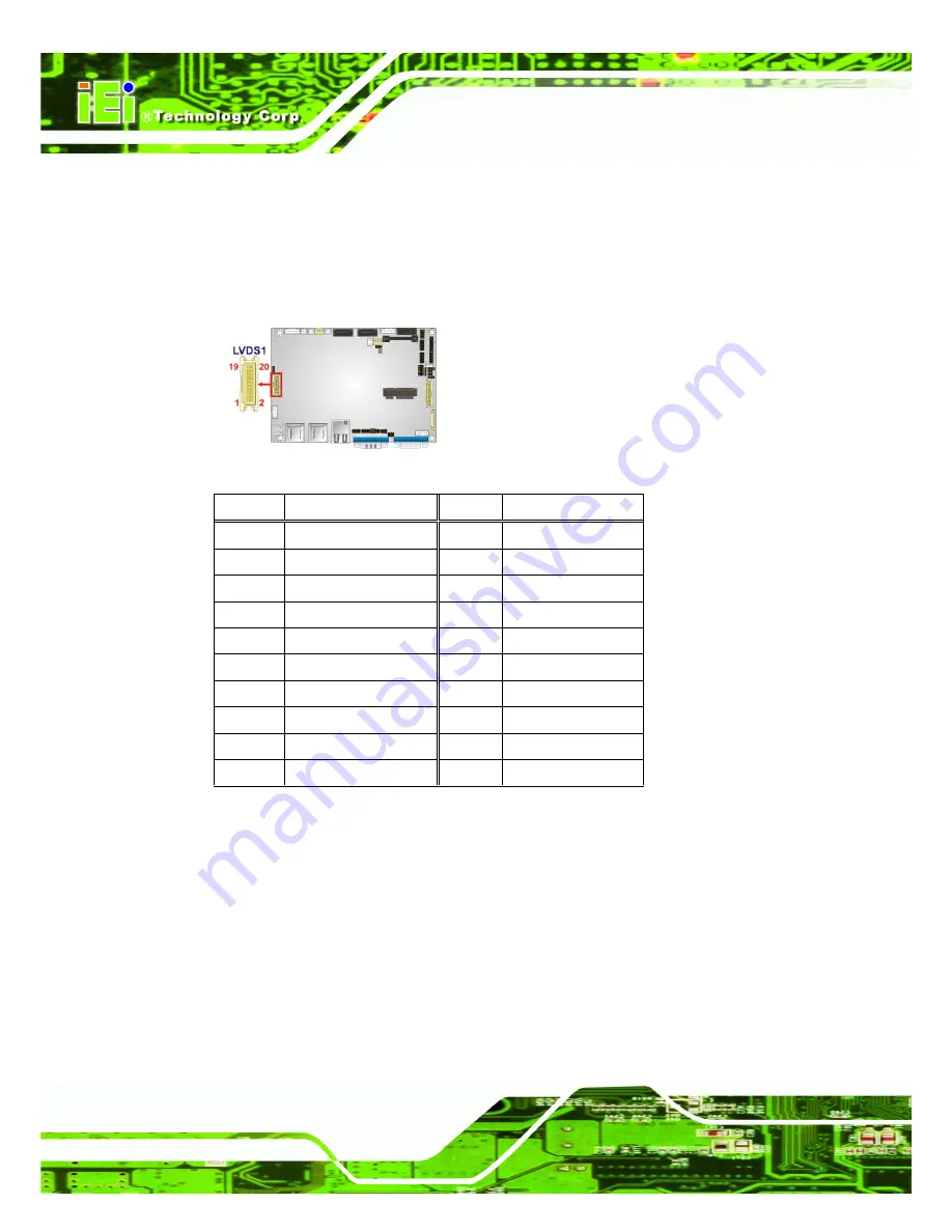
CN Type:
20-pin crimp
CN Location:
See
Figure 3-11
CN Pinouts:
See
Table 3-12
The LVDS connector is for an LCD panel connected to the board.
Figure 3-11: LVDS Connector Location
Pin
Description
Pin
Description
1
GND1
2
GND2
3
A_Y0
4
A_Y0#
5
A_Y1
6
A_Y1#
7
A_Y2
8
A_Y2#
9
A_CK
10
A_CK#
11
NC
12
NC
13
GND3
14
GND4
15
NC
16
NC
17
VCC_LCD
18
VCC_LCD
19
VCC_LCD
20
VCC_LCD
Table 3-12: LVDS Connector Pinouts
3.2.11 LVDS2 Connector
CN Label:
LVDS2
CN Type:
30-pin crimp
CN Location:
See
Figure 3-11
CN Pinouts:
See
Table 3-12
The LVDS2 connector is for an LCD panel connected to the board.
Summary of Contents for WAFER-PV-D4253
Page 14: ......
Page 15: ...WAFER PV D5253 D4253 N4553 SBC Page 1 Chapter 1 1 Introduction...
Page 23: ...WAFER PV D5253 D4253 N4553 SBC Page 9 Chapter 2 2 Packing List...
Page 27: ...WAFER PV D5253 D4253 N4553 SBC Page 13 Chapter 3 3 Connectors...
Page 54: ...WAFER PV D5253 D4253 N4553 SBC Page 40 Chapter 4 4 Installation...
Page 78: ...WAFER PV D5253 D4253 N4553 SBC Page 64 Chapter 5 5 BIOS...
Page 102: ...WAFER PV D5253 D4253 N4553 SBC Page 88 Appendix A A BIOS Options...
Page 105: ...WAFER PV D5253 D4253 N4553 SBC Page 91 Appendix B B One Key Recovery...
Page 133: ...WAFER PV D5253 D4253 N4553 SBC Page 119 Appendix C C Terminology...
Page 137: ...WAFER PV D5253 D4253 N4553 SBC Page 123 Appendix D D Hazardous Materials Disclosure...