


NOVA-PV-D5251/D4251 5.25" SBC
Page 178
此附件旨在确保本产品符合中国
RoHS
标准。以下表格标示此产品中某有毒物质的含量符
合中国
RoHS
标准规定的限量要求。
本产品上会附有
”
环境友好使用期限
”
的标签,此期限是估算这些物质
”
不会有泄漏或突变
”
的
年限。本产品可能包含有较短的环境友好使用期限的可替换元件,像是电池或灯管,这些元
件将会单独标示出来。
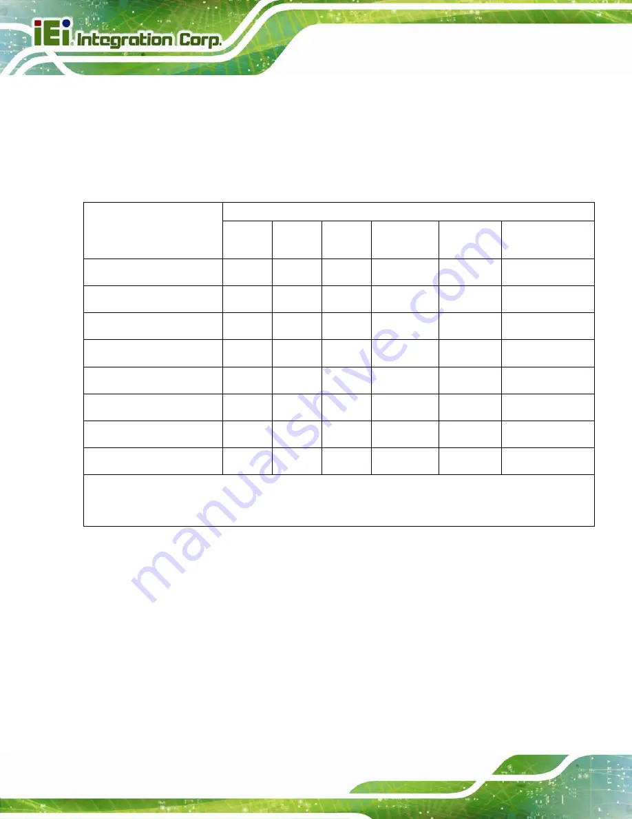
有毒有害物质或元素
部件名称
铅
(Pb)
汞
(Hg)
镉
(Cd)
六价铬
(CR(VI))
多溴联苯
(PBB)
多溴二苯醚
(PBDE)
壳体
X
O O O
O
X
显示
X
O O O
O
X
印刷电路板
X
O O O
O
X
金属螺帽
X
O O O
O
O
电缆组装
X
O O O
O
X
风扇组装
X
O O O
O
X
电力供应组装
X
O O
O
O
X
电池
O
O O O
O
O
O:
表示该有毒有害物质在该部件所有物质材料中的含量均在
SJ/T11363-2006
标准规定的限量要求以下。
X:
表示该有毒有害物质至少在该部件的某一均质材料中的含量超出
SJ/T11363-2006
标准规定的限量要求。
Summary of Contents for NOVA-PV-D5251
Page 16: ......
Page 17: ...NOVA PV D5251 D4251 5 25 SBC Page 1 1 Introduction Chapter 1...
Page 21: ...NOVA PV D5251 D4251 5 25 SBC Page 5 Figure 1 3 Connector Solder Side...
Page 23: ...NOVA PV D5251 D4251 5 25 SBC Page 7 Figure 1 5 NOVA PV D5251 D4251 Dimensions mm...
Page 28: ...NOVA PV D5251 D4251 5 25 SBC Page 12 2 Unpacking Chapter 2...
Page 33: ...NOVA PV D5251 D4251 5 25 SBC Page 17 3 Connectors Chapter 3...
Page 77: ...NOVA PV D5251 D4251 5 25 SBC Page 61 4 Installation Chapter 4...
Page 106: ...NOVA PV D5251 D4251 5 25 SBC Page 90 5 BIOS Screens Chapter 5...
Page 138: ...NOVA PV D5251 D4251 5 25 SBC Page 122 Appendix A A BIOS Menu Options...
Page 141: ...NOVA PV D5251 D4251 5 25 SBC Page 125 Appendix B B One Key Recovery...
Page 149: ...NOVA PV D5251 D4251 5 25 SBC Page 133 Figure B 5 Partition Creation Commands...
Page 183: ...NOVA PV D5251 D4251 5 25 SBC Page 167 Appendix C C Terminology...
Page 188: ...NOVA PV D5251 D4251 5 25 SBC Page 172 Appendix D D Watchdog Timer...
Page 191: ...NOVA PV D5251 D4251 5 25 SBC Page 175 Appendix E E Hazardous Materials Disclosure...


