background image

CLOUD


47

X

0


F


R

EFERENCE 

M

ANUAL


86 


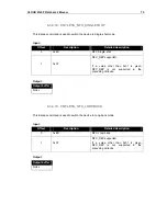
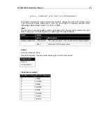
6.3.5.10.  CONTACT_GET_SET_MCARD_TIMEOUT 


This Escape command is used to get or set the delay which is applied after a Write operation to 
memory cards. The delay is specified in milliseconds. 

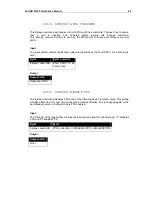
Input: 

The  first  byte  of  the  input  buffer  will  contain  the  Escape  code;  the  next  byte  will  contain  the 
memory card write delay in seconds. 


Output: 

Write delay: No response byte 

Read delay value: A byte value specifying the current delay applied during memory card Write 
in milliseconds 


Byte0 

Byte1 

Value 

Description 


Escape 
code(0x85) 


0x01 


Delay in milliseconds for memory card Write 


Any value other than 


Read  the  current  applied  delay  for  memory  card 
Write 


Byte0 

Null or 

Delay in ms 

Summary of Contents for CLOUD 47x0 F

Page 1: ...Identive Infrastructure Reference Manual version 1 0 CLOUD 47x0 F Dual Interface Smartcard Readers ...

Page 2: ...Reference manual CLOUD 47x0 F Dual Interface Smartcard Readers Identive GmbH Oskar Messter Strasse 13 85737 Ismaning Germany Phone 49 89 9595 5000 Fax 49 89 9595 5555 ...

Page 3: ...Document history Date Version Description of change 01 24 2013 1 0 Initial Version Contact information CLOUF 4700 F CLOUD 4710F For sales information please email sales identive infrastructure com ...

Page 4: ... F customization options 15 3 6 Contactless communication principles and CLOUD 47x0 F usage recommendations16 3 6 1 Power supply 16 3 6 2 Data exchange 16 3 6 3 Recommendations 17 3 7 Applications 17 3 7 1 General 17 3 7 2 Applications provided by Identive GmbH 18 4 CLOUD 47x0 F characteristics 19 4 1 CLOUD 47x0 F high level architecture 19 4 1 1 Block diagram 19 4 1 2 Software architecture 20 4 2...

Page 5: ...IFARE_VALUE_BLK_NEW 40 6 2 10 PAPDU_TCL_PASS_THRU T CL Pass Thru 41 6 2 11 PAPDU_ISO14443_PART3_PASS_THRU Mifare Pass Thru 42 6 2 12 PAPDU_ISO14443_PART4_PART3_SWITCH TCL Mifare Switch 42 6 2 13 PAPDU_FELICA_REQC 43 6 2 14 PAPDU_FELICA_REQ_SERVICE 43 6 2 15 PAPDU_FELICA_REQ_RESPONSE 44 6 2 16 PAPDU_FELICA_READ_BLK 44 6 2 17 PAPDU_FELICA_WRITE_BLK 45 6 2 18 PAPDU_FELICA_SYS_CODE 45 6 2 19 PAPDU_NFC...

Page 6: ...P_TARGET_RECEIVE 72 6 3 4 15 CNTLESS_P2P_TARGET_SEND 73 6 3 4 16 CNTLESS_P2P_INITIATOR_DESELECT 73 6 3 4 17 CNTLESS_P2P_INITIATOR_TRANCEIVE 74 6 3 4 18 CNTLESS_NFC_SINGLESHOT 75 6 3 4 19 CNTLESS_NFC_LOOPBACK 75 6 3 4 20 CNTLESS_GET_SET_NFC_PARAMS 76 6 3 4 21 CNTLESS_GET_P2P_EXTERNAL_RF_STATE 77 6 3 5 Specific for Contact Interface 78 6 3 5 1 CONTACT_GET_SET_PWR_UP_SEQUENCE 79 6 3 5 2 CONTACT_EMV_L...

Page 7: ...us words table 91 7 2 Annex B Sample code using escape commands 92 7 3 Annex C Mechanical drawings 95 7 3 1 Outline and cable positions 95 7 3 2 Stand 96 7 3 3 Reader mounted to Stand 97 7 3 4 CLOUD 4710 F SAM slot 98 ...

Page 8: ......

Page 9: ...ice problems with the provided documentation please provide your feedback to support identive group com 1 2 Licenses If the document contains source code examples they are provided for illustrative purposes only and subject to the following restrictions You MAY at your own risk use or modify the source code provided in the document in applications you may develop You MAY distribute those applicati...

Page 10: ...ported commands available for developers using CLOUD47x0 F in their applications 2 2 Target audience This document describes the technical implementation of CLOUD 47x0 F The manual targets software developers It assumes knowledge about ISO 7816 13 56 MHz contactless technologies like ISO IEC 14443 and commonly used engineering terms Should you have questions you may send them to support identive g...

Page 11: ...A with extensions for security NXP NA Not applicable NAD Node Address Nibble Group of 4 bits 1 digit of the hexadecimal representation of a byte Example 0xA3 is represented in binary as 10100011 b The least significant nibble is 0x3 or 0011 b and the most significant nibble is 0xA or 1010 b PCD Proximity Coupling Device PC SC Personal Computer Smart Card software interface to communicate between a...

Page 12: ...or ICCs and Personal Computer Systems v2 01 PC SC Workgroup PCSC3 Interoperability Specification for ICCs and Personal Computer Systems Part 3 Requirements for PC Connected Interface Devices PC SC Workgroup PCSC3 AMD1 Interoperability Specification for ICCs and Personal Computer Systems Part 3 Requirements for PC Connected Interface Devices Amendment 1 PC SC Workgroup PCSC3 SUP Interoperability Sp...

Page 13: ...4 B5 B6 B7 B8 B9 B10 B11 B0 B1 B2 B3 Least significant nibble Most significant nibble 1 Byte 8 bits 2 nibbles Bit number 0 Bit number 5 String of 12 bytes Byte number 11 Byte number 2 Example 163 decimal number is represented in hexadecimal as 0xA3 in binary as 10100011 b The least significant nibble of 0xA3 is 0x3 in hexadecimal 0011 b in binary The most significant nibble of xA3 is 0xA in hexade...

Page 14: ...OUD 47x0 F key features 13 56MHz contactless reader o ISO14443 type A B o MIFARETM ISO7816 compliant contact smart card reader for ID 1 cards CLOUD 4700 F ISO7816 compliant contact smart card reader for ID 000 cards CLOUD 4710 F PC SC v2 0 compliant Full CCID for both the contact and the contactless interfaces Secure in field SmartOSTM firmware upgrade Unique reader serial number which enables tha...

Page 15: ...on the desktop with an angle of 40 in regard to the desk or to mount it to a wall with a 40 angle in regard to that The wireholder keeps the contactless token in place when using this option 3 5 CLOUD 47x0 F customization options Upon request Identive GmbH can consider customizing The color of the casing The logo The product label The USB strings Terms and conditions apply please contact your loca...

Page 16: ...uples with the reader and an induction current appears in the antenna thus providing power to the integrated circuit The generated current is proportional to the magnetic flux going through the antenna of the user credential 3 6 2 Data exchange The carrier frequency of the magnetic field is used as a fundamental clock signal for the communication between the reader and the credential It is also us...

Page 17: ... size of the reader s and credential s antennas directly influence the inductive coupling and therefore the communication CLOUD 47x0 F was designed and optimized to function with user credentials of various technologies and sizes It may happen that CLOUD 47x0 F is not capable of communicating with extremely large or extremely small credentials In order to optimize the coupling between the reader a...

Page 18: ... applications or PKI or CAC applications Identive GmbH provides a few applications for development and evaluation purposes that can function with CLOUD 47X0 F There are many tools provided here are two of them The Simple NFC Tag Editor is part of our NFC NDEF Editor Kit that enables the user to read and write NFC forum compliant records from to NFC forum compatible tags It is an easy to use tool t...

Page 19: ...r LED for reader status indication A contact smart card interface An RF front end that handles the RF communication The controller embeds flash memory that contains the firmware developed by Identive to handle all the ISO7816 contact protocol the RF communication protocols and the PC SC communication protocol with the host The flash can be upgraded once the device is deployed in the field hence en...

Page 20: ...ly available for all supported operating systems Windows MacOSX and Linux With current Windows versions starting with Windows Vista and MacOSX this driver is already included in the basic installation With the diverse Linux derivatives there may be distribution specific drivers that should get installed using the install mechanism of the used distribution If there is none the driver may always be ...

Page 21: ... mm X 93 mm X 22 mm Cable length 1 5 meter long with USB type A connector Default color White and grey Default label CLOUD 4710 F Weight 157g without stand Stand 52g External dimensions 113 mm X 93 mm X 22 mm Cable length 1 5 meter long with USB type A connector Default color White and grey Default label Drawing with dimensions of the CLOUD 47X0 F and accessories can be found in annex ...

Page 22: ...ed ON ON Contact card powered communication 500ms ON 500ms OFF OFF Contactless card powered communication 500ms ON 500ms OFF 500ms ON 500ms OFF Reader card errors OFF 100ms ON 100ms OFF Dual interface card powered in contact Slot 500ms ON 500ms OFF OFF Dual interface card powered using RF field 500ms ON 500ms OFF 500ms ON 500ms OFF 4 2 3 Other data 4 2 3 1 General Parameter Value Description Clock...

Page 23: ...C Synchronous smart cards ISO 7816 compliant Yes CT API compliant Yes Number of slots Single smart card slot Ejection mechanism Manual 4 2 3 4 Contactless interface Parameter Value Description RF carrier frequency 13 56MHz 50ppm Maximum supported card baud rate 848Kbps Cards supported MIFARE Classic 1K and 4K DESFire DESFire EV1 Ultralight Ultralight C MIFARE mini and MIFARE Plus FeliCa 212 and 42...

Page 24: ...ed driver for this reader as well which is available through Windows Update or on the Identive support pages 5 2 Utilities The following utilities are available A tool for testing the resource manager A tool called PCSCDiag capable of providing basic information about the reader and a card through PC SC stack 5 3 Driver 5 3 1 CLOUD 47x0 F listing CLOUD 47X0 F is listed by PC SC applications as Ide...

Page 25: ... interpreted according to the Part 3 Supplemental Document maintained by PC SC Credentials using technology like MIFARE are examples of this Byte Value Designation Description 0 0x3B Initial header 1 0x8n T0 n indicates the number of historical bytes in following ATR 2 0x80 TD1 upper nibble 8 indicates no TA2 TB2 TC2 lower nibble 0 means T 0 3 0x01 TD2 upper nibble 0 indicates no TA3 TB3 TC3 lower...

Page 26: ...pper nibble 8 indicates no TA2 TB2 TC2 lower nibble 0 means T 0 3 0x01 TD2 upper nibble 0 indicates no TA3 TB3 TC3 lower nibble 1 means T 1 4 3 n Historical bytes or application information Type A the historical bytes from the ATS up to 15 bytes Type B 8 bytes Byte 0 through 3 application data from ATQB Byte 4 through 6 protocol info byte from ATQB Byte 7 highest nibble is the MBLI maximum buffer ...

Page 27: ... interface when received through bulk out endpoint PC_to_RDR_IccPowerOn PC_to_RDR_IccPowerOff PC_to_RDR_GetSlotStatus PC_to_RDR_XfrBlock PC_to_RDR_GetParameters PC_to_RDR_ResetParameters PC_to_RDR_SetParameters PC_to_RDR_Escape PC_to_RDR_ICCClock PC_to_RDR_T0APDU PC_to_RDR_Abort PC_to_RDR_SetDataRateAndClockFrequency 5 4 1 3 CCID Error Codes Extensive error codes are reported on many conditions du...

Page 28: ...eturned if the card is signaling to use a protocol other than T 0 or T 1 in its ATR 5 4 1 3 4 BAD_ATR_TS This error code is returned if the initial character of the ATR contains invalid data 5 4 1 3 5 BAD_ATR_TCK This error code is returned if the check character of the ATR contains is invalid 5 4 1 3 6 ICC_MUTE This error code is returned when the card does not respond until the reader time out o...

Page 29: ...U CLA INS P1 P2 Lc Data in Le 0xFF 0xCA 0x00 0x00 XX Setting Le 0x00 can be used to request the full UID or PUPI is sent back e g for ISO14443A single 4 bytes double 7 bytes triple 10 bytes for ISO14443B 4 bytes PUPI Response APDU Data Status Word Requested bytes of UID SW1 SW2 6 1 3 PAPDU_ESCAPE_CMD Usually escape commands are transmitted through SCardControl as defined in PCSC API using IOCTL_CC...

Page 30: ...APDU would be used Command APDU FF CC 00 00 02 01 01 to set to EMV mode Response APDU 90 00 Note 1 To send Escape commands using this method the reader should be connected in shared mode using T0 or T1 protocol Only then would the resource manager allow SCardTransmit 2 As the escape commands defined using READER_GENERIC_ESCAPE have ISO 7816 APDU format they can be sent using SCardTransmit without ...

Page 31: ... and P2 represent the block number of the block to be read starting with 0 for sector 0 block 0 continuing with 4 for sector 1 block 0 sector no x 4 block no Regardless of the value given in Le this command will always return the entire block content 16 bytes for Mifare Classic 4 bytes for Mifare UL and UL C Response APDU Data Status Word N bytes of block data SW1 SW2 Example For a Mifare Classic ...

Page 32: ... data For a description of P1 and P2 see PAPDU_MIFARE_READ_BINARY Lc has got to match the block size of the used card 16 bytes for Mifare Classic 4 bytes for Mifare UL and UL C Response APDU Data Status Word SW1 SW2 Example To write the bytes AA 55 AA 55 AA 55 AA 55 AA 55 AA 55 AA 55 AA 55 to block 7 of a Mifare Classic 1K the following command has got to be issued APDU FF D6 00 06 10 AA 55 AA 55 ...

Page 33: ...supported by CLOUD 47x0 F Notes 1 Card keys can be loaded in both secure and non secure mode Card keys can only be loaded to the Volatile memory of the reader 2 To load the card keys in secure mode the application developer has to know the 128 bit AES key of the reader The default key is 00010203 05060708 0A0B0C0D 0F101112 As a Mifare key is only 6 bytes in length data needs to be padded as per pk...

Page 34: ...0A AES128 Encrypted 10229E33 189403FD A9C14110 B1BB02B4 Load keys command FF82406010 10229E33 189403FD A9C14110 B1BB02B4 Load Keys Reader Secure If the default AES128 reader is key is 00010203 05060708 0A0B0C0D 0F101112 then the following explains the steps needed to change the reader key to 10111213 15161718 1A1B1C1D 1F202122 Reader old key A 00010203 05060708 0A0B0C0D 0F101112 Reader new key B 1...

Page 35: ...x the data structure is defined as follows Byte Value Description B0 0x01 Version B1 Block Number MSB always 0x00 for Mifare Classic cards B2 Block Number LSB B3 0x60 Mifare Classic Key A 0x61 Mifare Classic Key B B4 Key number shall be set to 0x01 Response APDU Data Status Word SW1 SW2 Example Load Key A unencrypted and authenticate for block 6 sector 1 actually with that key APDU FF 82 00 60 06 ...

Page 36: ...ad from card Mifare UL Entire card data is returned 64 bytes SW1 SW2 Example Read sector 1 of a Mifare Classic 1K APDU FF B1 00 01 00 SW12 9000 OK DataOut 00 00 00 00 00 00 00 00 00 00 00 00 00 00 00 00 00 01 02 03 04 05 06 07 08 09 0A 0B 0C 0D 0E 0F AA 55 AA 55 AA 55 AA 55 AA 55 AA 55 AA 55 AA 55 48 bytes Read entire content of a Mifare UL APDU FF B1 00 01 10 SW12 9000 OK DataOut 04 6B 5D BA 09 F...

Page 37: ...a Read Sector Extended FF B3 Addr MSB Addr LSB 0 Response APDU Data Status Word Mifare classic 64 bytes of sector data read from card Mifare UL Entire card data is returned 64 bytes SW1 SW2 Example Read sector 1 of a Mifare Classic 1K APDU FF B3 00 01 10 SW12 9000 OK DataOut 00 00 00 00 00 00 00 00 00 00 00 00 00 00 00 00 00 01 02 03 04 05 06 07 08 09 0A 0B 0C 0D 0E 0F AA 55 AA 55 AA 55 AA 55 AA 5...

Page 38: ...a Mifare Classic and 0xF0 when writing to the large sectors of a Mifare Classic 4K Lc has got to be 0x30 for Mifare UL and the data will get written from block 4 till the end of the memory Response APDU Data Status Word SW1 SW2 6 2 8 PAPDU_MIFARE_VALUE_BLK_OLD This command increments or decrements the data in a Value Block on a Mifare Classic card Command APDU Command CLA INS P1 P2 P3 Data Increme...

Page 39: ...value block prior to executing this command see datasheet for Mifare Classic cards APDU FF B0 00 04 00 Read Block 4 SW12 9000 OK DataOut A9 AA AA AA 56 55 55 55 A9 AA AA AA 05 FA 05 FA 16 bytes APDU FF F0 00 04 06 C0 04 01 00 00 00 decrement block 4 by 1 SW12 9000 OK APDU FF B0 00 04 00 Read Block 4 SW12 9000 OK DataOut A8 AA AA AA 57 55 55 55 A8 AA AA AA 05 FA 05 FA 16 bytes ...

Page 40: ...ormed which block the actions pertain to the destination s and which value should be applied for the action Tags for the action include 0xA0 Increment 0xA1 Decrement The Tag to define the destination is 0x80 Destination The Tag to define the value is 0x81 value to increment or decrement Destination by LSB first Example Increment block 5 by 100 FF C2 00 03 0B A0 09 increment 80 01 05 block 5 81 04 ...

Page 41: ...Data object XX with unexpected length XX 6A 80 Data object XX with unexpected vale XX 64 00 Data Object XX execution error no response from IFD XX 64 01 Data Object XX execution error no response from ICC XX 6F 00 Data object XX failed no precise diagnosis 6 2 10 PAPDU_TCL_PASS_THRU T CL Pass Thru This command can be used to send raw data using T CL protocol to a card Please refer to the status wo...

Page 42: ...bytes Response APDU Data Status Word Data returned by card SW1 SW2 6 2 12 PAPDU_ISO14443_PART4_PART3_SWITCH TCL Mifare Switch This command switches the card state between TCL and MIFARE modes Command APDU Command CLA INS P1 P2 P3 Data Part 4 Part 3 Switch FF F8 P1 00 00 P1 0x00 switches from MIFARE mode to TCL mode P1 0x01 switches from TCL mode to MIFARE mode Response APDU Data Status Word SW1 SW...

Page 43: ...stem Code sent only if the RFU byte is 0x01 SW1 SW2 6 2 14 PAPDU_FELICA_REQ_SERVICE This command issues a REQ SERVICE as defined in JIS 9 6 2 P1 On receiving this command an NFC Forum tag type 3 will respond with the area key version of the specified area and the service key version of the specified service Command APDU Command CLA INS P1 P2 P3 Data FeliCa REQ Service FF 42 Number of services area...

Page 44: ... PAPDU_FELICA_READ_BLK This command issues a READ as defined in JIS 9 6 3 P1 specifies the number of service P2 specifies the number of blocks Data buffer specifies the service code and block list When an NFC Forum tag type 3 receives this command it responds with the record value of the specified service Command APDU Command CLA INS P1 P2 P3 Data FeliCa REQ Response FF 46 Number of service Number...

Page 45: ...S P1 P2 P3 Data FeliCa Write Block 0xFF 0x48 Number of service Number of blocks 2 P1 P2 16 P2 Service Code List Block List Block Data Response APDU Data Status Word 8 bytes IDm Status Flag 1 Status Flag 2 SW1 SW2 6 2 18 PAPDU_FELICA_SYS_CODE This command issues a REQ SYSTEM CODE as defined in RC S850 860 Command Ref Manual Section 6 1 7 Command APDU Command CLA INS P1 P2 P3 Data FeliCa REQ SYSTEM ...

Page 46: ...ytes Header ROM which identify the tag UID0 through UID3 are the first 3 bytes of the tag s UID Topaz tags have a 7 bytes long UID which can be fully fetched using the GET_UID APDU described earlier in this manual 6 2 20 PAPDU_NFC_TYPE1_TAG_RALL This command issues a RALL to read the two header ROM bytes and the whole of the static memory blocks 0x0 0xE Command APDU Command CLA INS P1 P2 P3 Data T...

Page 47: ...e within the block value between 0 and 7 Response APDU Data Status Word Data returned by card SW1 SW2 6 2 22 PAPDU_NFC_TYPE1_TAG_WRITE_E This command issues a WRITE to erase and then write the value of 1 memory byte within the static memory model area of blocks 0x0 0xE Command APDU Command CLA INS P1 P2 P3 Data TYPE1 Tag WRITE ERASE FF 56 00 Byte Addr 01 Data Where P2 codes the address of the memo...

Page 48: ... command for NFC Forum tags type 1 is approximately half that of the normal write command WRITE E Using this command EEPROM bits can only be set not reset Command APDU Command CLA INS P1 P2 P3 Data TYPE1 Tag WRITE No ERASE FF 58 00 Byte Addr 01 Data Where P2 codes the address of the memory byte in the following way Bit numbers Description b7 b3 Block value between 0x0 and 0xE b2 b0 Byte within the...

Page 49: ...gAddr 00 Where P2 Segment Address is Bit numbers Description b7 b4 Segment 0x0 0xF b2 b0 0 Response APDU Data Status Word 128 bytes of data SW1 SW2 6 2 25 PAPDU_NFC_TYPE1_TAG_READ8 This command issues a READ8 to read out a block of eight bytes Please note that this command only works on Topaz tags in dynamic memory model Command APDU Command CLA INS P1 P2 P3 Data TYPE1 Tag READ BLOCK FF 5C 00 Bloc...

Page 50: ...PDU Data Status Word 8 bytes of data that have been written SW1 SW2 6 2 27 PAPDU_NFC_TYPE1_TAG_WRITE_NE8 This command issues a WRITE8 to write a block of eight bytes It does not erase the value of the targeted byte before writing the new data Using this command EEPROM bits can be set but not reset Please note that this command only works on Topaz tags in dynamic memory model Command APDU Command C...

Page 51: ...order to be able to send Escape commands for the CLOUD 47x0 F the feature has got to be enabled by setting a REG_DWORD value named EscapeCommandEnable in the registry to a value of 1 For Windows XP and Windows Vista the key to hold the value would be HKEY_LOCAL_MACHINE SYSTEM CurrentControlSet Enum USB VID_04E6 PID_58 10 Device Instance xxxx Device Parameters For Windows 7 and Windows 8 that would...

Page 52: ...ER_SETMODE 0x01 READER_GETMODE 0x02 READER_GETIFDTYPE 0x12 READER_LED_CONTROL 0x19 READER_GETINFO_EXTENDED 0x1E READER_LED_CONTROL_BY_FW 0xB2 READER_RDWR_USR_AREA 0xF0 READER_GENERIC_ESCAPE FF 70 04 E6 XX 6 3 3 1 READER_SETMODE This Escape command sets the current mode of the reader Applications may call this function to set the desired mode Typically this call is used to switch between the ISO781...

Page 53: ...DR_ICCPOWEROFF 0x63 Output Output buffer NULL 6 3 3 2 READER_GETMODE This Escape command retrieves the current mode of the reader Input The input buffer contains the escape code value Output The currently active reader mode will be returned as a byte value Mode Value Remarks ISO 0x00 ISO 7816 mode EMV 0x01 EMV mode Synchronous 0x02 Memory card mode synchronous NFC Test 0x04 NFC Test Mode Mode Valu...

Page 54: ... Reader 0x50 0x57 Identive CLOUD 2910 F Smart Card Keyboard Reader 6 3 3 4 READER_LED_CONTROL This Escape command is used to toggle the LED state LED control by firmware should be disabled using the escape command READER_LED_CONTROL_BY_FW to see proper LED change when using this IOCTL Input The first byte of the input buffer contains the escape code followed by LED number if more than one LED is p...

Page 55: ...bySupportedModes Bit map indicating the supported modes of the reader 0x01 EMV mode 0x02 Memory card mode 0x04 Nfc test mode 0x07 for Contact Contactless readers 0x03 for Contact only readers Note ISO mode is not indicated as it is always supported 2 wSupportedProtocols Protocols supported by the Reader Bit 0 T0 Bit 1 T1 0x0003 Received as LSB first 2 winputDevice IO_DEV_NONE 0x00 IO_DEV_KEYPAD 0x...

Page 56: ...d in the non volatile memory of the reader and hence data will be retained even after power cycle Note Frequent writes should be avoided The non volatile memory supports only 100K writing cycles A maximum of 249 bytes can be read and written The sector can be read and written only as a whole If complete data 249 bytes is not given during write operation then random data will be padded to the given...

Page 57: ... to identify the specific command Byte0 Byte1 Byte2 Byte3 Byte4 From Byte5 up to Lc bytes ByteLc 5 Byte 5 Byte 6 onwards 0xFF 0x70 0x04 0xE6 Lc always 0 Cmd Opcode Command parameters or data Le optional Output Depending on the command the output shall be Le bytes of data SW1 SW2 or SW1 SW2 The escape message shall at least return 2 bytes status word SW1 SW2 In case of success SW1 0x90 and SW2 0x00...

Page 58: ... used along with CNTLESS_ SWITCH_RF_ON_OFF Input To Enable Disable Get Current Status of Contact Slot Byte0 CLA Byte1 INS Byte2 P1 Byte3 P2 Byte4 Lc Byte5 Byte6 Byte7 Le 0xFF 0x70 0x04 0xE6 0x03 0x05 opcode 0x01 0x01 to enable 00 0x00 to disable 0xFF 0x70 0x04 0xE6 0x02 0x05 opcode 0x00 to get current contact status 00 Byte2 and Byte3 constitute the world wide unique vendor ID as assigned by the U...

Page 59: ...ETECTED 0xE4 CNTLESS_FELICA_PASS_THRU 0xF3 CNTLESS_P2P_SWITCH_MODES 0xE9 CNTLESS_P2P_TARGET_RECEIVE 0xEA CNTLESS_P2P_TARGET_SEND 0xEB CNTLESS_P2P_INITIATOR_DESELECT 0xE6 CNTLESS_P2P_INITIATOR_TRANSCEIVE 0xE7 CNTLESS_NFC_SINGLESHOT 0xEC CNTLESS_NFC_LOOPBACK 0xED CNTLESS_GET_SET_NFC_PARAMS READER_ESCAPE_GENERIC 0x04 CNTLESS_GET_P2P_EXTERNAL_RF_STATE READER_ESCAPE_GENERIC 0x06 6 3 4 1 CNTLESS_GET_CAR...

Page 60: ...direction reader to card b2 848kbps supported direction reader to card b3 always 0 b4 212kbps supported direction card to reader b5 424kbps supported direction card to reader b6 848kbps supported direction card to reader b7 1 indicates same baud rate in both directions 0 indicates different baud rates in both directions Example If 0xNN 0x77 the card supports all baud rates namely 106 212 424 and 8...

Page 61: ...PPS This Escape command disables the automatic PPS done by the firmware device for contactless cards Input The first byte of input buffer contains the escape code The second byte either sets the mode or contains a code to retrieve the setting Output No response is returned for set state For Get State 1 byte response is received Output buffer NULL or current state Byte0 Escape code 0x93 Input Outpu...

Page 62: ... in the reader the RF field is turned OFF Input The first byte of input buffer contains the escape code The second byte either sets the mode or contains a code to retrieve the setting After the RF is turned off to turn the RF ON again card connect has to be done in direct mode Byte0 Byte1 Output Value Description Byte0 Escape code 0x96 0x00 Switch RF Field OFF No Output 0x01 Switch RF Field ON No ...

Page 63: ...6Kbps from PICC to PCD 424Kbps from PCD to PICC 0x03 106Kbps from PICC to PCD 848Kbps from PCD to PICC 0x10 212Kbps from PICC to PCD 106Kbps from PCD to PICC 0x11 212Kbps in both directions 0x12 212Kbps from PICC to PCD 424Kbps from PCD to PICC 0x13 212Kbps from PICC to PCD 848Kbps from PCD to PICC 0x20 424Kbps from PICC to PCD 106Kbps from PCD to PICC 0x21 424Kbps from PICC to PCD 212Kbps from PC...

Page 64: ...ains the escape code The second byte either sets the mode or contains a code to retrieve the setting Output No response is returned for set state For Get State 1 byte response is received Output buffer NULL or current state Input Output Byte0 Byte1 Description Byte 0 Escape code 0xA7 0x00 Enable RNAK retries No Output 0x01 Disable RNAK retries No Output 0xFF Get current state of retries 0x00 Retri...

Page 65: ...is returned for set state For Get State 1 byte response is received Output buffer NULL or current state 6 3 4 9 CNTLESS_GET_CARD_DETAILS This Escape command is used to get details about the PICC placed in the field of the reader Input The first byte of input buffer contains the escape code Input Output Byte0 Byte1 Description Byte 0 Escape code 0xAC 0x00 Enable polling No output 0x01 Disable polli...

Page 66: ... PUPI UID bytes 0x00 byte padding used if length smaller than 10 B13 0x00 CID not supported 0x01 CID supported B14 0x00 NAD not supported 0x01 NAD supported B15 Bit Rate Capability B16 FWI B17 IFSC B18 MBLI B19 SAK B20 SFGI OR B3 B10 8 Bytes NFCID2 B11 Request service command response time parameter see JIS 6319 specification B12 Request response command response time parameter B13 Authentication ...

Page 67: ... Type A RXGAIN for polling or 106Kbps B2 Type A RXGAIN for 212 Kbps B3 Type A RXGAIN for 424 Kbps B4 Type A RXGAIN for 848 Kbps B5 Type A RX THRESHOLD for polling or 106Kbps B6 Type A RX THRESHOLD for 212 Kbps B7 Type A RX THRESHOLD for 424 Kbps B8 Type A RX THRESHOLD for 848 Kbps B9 Type B RXGAIN for polling or 106Kbps B10 Type B RXGAIN for 212 Kbps B11 Type B RXGAIN for 424 Kbps B12 Type B RXGAI...

Page 68: ...ough to send FeliCa commands to FeliCa cards Input The first byte of input buffer contains the escape code followed by FeliCa command to be sent to the card At least 1 byte of command is required to be sent to the card Otherwise an error will be reported Output The response received from the FeliCa card is sent as output for this escape command Byte0 Escape code 0xE4 Byte0 Value Description 0x00 C...

Page 69: ... mode or contains a code to retrieve the setting Additional data bytes will be needed for Initiator Target mode Offset Description Detailed description 0 0xE9 Switch mode 1 0 P2P Initiator mode 1 P2P Target mode 2 Reader writer mode 0xFF Get current mode For the switch to Initiator Target mode the bytes from offset 0x02 give additional information as described below Offset Initiator Mode Bytes Det...

Page 70: ...A6 NFCID2 16 0xC9 NFCID2 17 0x89 NFCID2 18 C0 FeliCa Padding Bytes 19 C1 FeliCa Padding Bytes 20 C2 FeliCa Padding Bytes 21 C3 FeliCa Padding Bytes 22 C4 FeliCa Padding Bytes 23 C5 FeliCa Padding Bytes 24 C6 FeliCa Padding Bytes 25 C7 FeliCa Padding Bytes 26 FF FeliCa System Code 27 FF FeliCa System Code 28 0x00 NFCID3 XOR of 0x08 and 3 bytes of NFCID1 29 0x88 Timeout Low Byte 30 0x13 Timeout High...

Page 71: ...st computer Target Mode On successful detection by the initiator the entire ATR_REQ buffer from the initiator device would be given to the host computer Reader Mode The output buffer would be empty Get Current Mode A single byte response indicating the currently selected mode as described below o 0x00 P2P Initiator mode o 0x01 P2P Target mode o 0x02 Reader Writer mode ...

Page 72: ...P_SWITCH_MODES E9 Input Buffer Offset Description Detailed description 0 0xEA Target Receive 1 RFU 2 RFU 3 RFU 4 0 No Chaining 1 Chaining Chaining byte 5 Timeout Low Byte 6 Timeout High Byte Output Buffer On successful reception the entire data from the initiator device would be returned from offset 0x04 Offset Description Detailed description 0 RFU 1 RFU 2 RFU 3 0 No Chaining 1 Chaining Chaining ...

Page 73: ...6 Timeout High Byte Offset 7 to offset 7 N N data bytes Bytes to be sent to Initiator device Output Once the data bytes are sent successfully the firmware would indicate if it is ready to send more bytes through the chaining byte Offset Description Detailed description 0 RFU 1 RFU 2 RFU 3 0 No Chaining 1 Chaining Chaining 6 3 4 16 CNTLESS_P2P_INITIATOR_DESELECT This escape command is used by the a...

Page 74: ...0xE7 Initiator transceive 1 0x00 RFU 2 0x00 RFU 3 0x00 RFU 4 0 No Chaining 1 Chaining Chaining 5 Timeout Low Byte 6 Timeout High Byte Offset 7 to 7 N N bytes of data Bytes to be sent to target device Output On successful reception of data from the target the entire data would be available from offset 0x04 Presence of additional data is indicated by the chaining byte Offset Description Detailed des...

Page 75: ...pported If a value other than 0x01 is given NFC_DEP is not supported in the preceding I Blocks Output Output buffer NULL 6 3 4 19 CNTLESS_NFC_LOOPBACK This Escape command is used to switch the device to Loop back mode Input Offset Description Detailed description 0 0xED NFC Loop back 1 0x01 NFC_DEP supported If a value other than 0x01 is given NFC_DEP is not supported in the preceding I Blocks Out...

Page 76: ...e1 INS Byte2 P1 Byte3 P2 Byte4 Lc Byte5 Byte6 Byte7 Byte 8 Le 0xFF 0x70 0x04 0xE6 0x04 0x04 opcode 0x01 SET NFC Parameter Value 00 To get the parameters the command syntax is Byte0 CLA Byte1 INS Byte2 P1 Byte3 P2 Byte4 Lc Byte5 Byte6 Byte7 Le 0xFF 0x70 0x04 0xE6 0x03 0x04 opcode 0x00 GET NFC Parameter 00 The value of byte 7 is interpreted from this table Byte 7 Value Description 0x00 DID Device Id...

Page 77: ...he reader got detected in target mode Input Byte0 CLA Byte1 INS Byte2 P1 Byte3 P2 Byte4 Lc Byte5 Le 0xFF 0x70 0x04 0xE6 0x01 0x06 opcode 00 Output If the command is successful a single byte is returned This byte indicates the value of parameter Bit 0 Set to logic 1 when a present external RF field is switched off Bit 1 Set to logic 1 when an external RF field is detected Bit 2 to Bit 7 RFU bits al...

Page 78: ...V_SINGLEMODE 0x06 CONTACT_EMV_TIMERMODE 0x07 CONTACT_APDU_TRANSFER 0x08 CONTACT_DISABLE_PPS 0x0F CONTACT_EXCHANGE_RAW 0x10 CONTACT_GET_SET_CLK_FREQUENCY 0x1F CONTACT_CONTROL_ATR_VALIDATION 0x88 CONTACT_GET_SET_MCARD_TIMEOUT 0x85 CONTACT_GET_SET_ETU 0x80 CONTACT_GET_SET_WAITTIME 0x81 CONTACT_GET_SET_GUARDTIME 0x82 CONTACT_READ_INSERTION_COUNTER READER_ESCAPE_GENERIC 0x00 ...

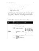
Page 79: ... card communication at that voltage If power up fails in all the enabled operating voltages then the firmware will report an error Input The first byte of the input buffer will contain the escape code The next byte shall contain the function to be performed Third byte shall contain the parameter for the function Byte0 Byte1 Byte2 Value Description Escape code 0x04 0x00 Starts with Class C voltage ...

Page 80: ...on Input The input buffer contains the escape code value Output Output buffer NULL Byte0 Byte 1 Byte2 Value Description 0x00 Starts with Class C voltage 1 8V 3V 5V order Time delay between resets in milliseconds Bit Map of all Voltage Classes Bit0 Class A Bit1 Class B Bit2 Class C 0x01 Starts with Class A voltage 5V 3V 1 8V order Byte0 Value Description 0x00 Starts with Class C voltage 1 8V 3V 5V ...

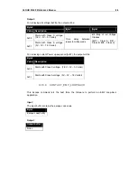
Page 81: ...Level 1 Testing Requirements document Input Output Output buffer NULL 6 3 5 4 CONTACT_EMV_TIMERMODE This Escape command lets the host perform a timer mode EMV Loop back application as specified in the EMV Level 1 Testing Requirements document Input The input buffer contains the escape code value Output Output buffer NULL Byte0 Escape code 0x06 Byte0 Escape code 0x07 ...

Page 82: ...the card Output Output buffer Response APDU 6 3 5 6 CONTACT_DISABLE_PPS This Escape command disables PPS done by the firmware device for smart cards This setting will take effect from the next card connect and remains effective till it is changed again or the next Reader power on Default mode is PPS enabled Input The first byte of the input buffer contains the Escape code and the following byte if...

Page 83: ...on any reception error Input The input buffer for this command contains the Escape code low byte of the length of data to be sent high byte of length of data to be sent low byte of the length of expected data high byte of length of expected data and the command Output Output buffer Response APDU Byte0 Byte1 Byte2 Byte3 Byte4 Byte 5 onwards Escape code 0x10 LSB of send length MSB of send length LSB...

Page 84: ...tains the Escape code the next byte contains the clock divisor value to set the clock frequency or 0xFF to get the clock frequency Output Set clock frequency None Get clock frequency One byte value indicating the current Clock divisor Output buffer NULL or current divisor Clock Divisor values DIVISOR VALUE SCCLK Frequency 12 4 MHz 10 4 8 MHz 8 6 MHz 7 6 8 MHz 6 8 MHz 5 9 6 MHz 4 12 MHz 3 16 MHz By...

Page 85: ...liant the card reader may fail to power up the card In these cases disabling ATR validation will let you work with the card regardless of ISO conformity of the ATR By default ATR validation is enabled Input The first byte of the input buffer will contain the Escape code the next byte will contain the control byte Output Output buffer NULL Byte0 Byte1 Value Description Escape code 0x88 0x00 Enable ...

Page 86: ...input buffer will contain the Escape code the next byte will contain the memory card write delay in seconds Output Write delay No response byte Read delay value A byte value specifying the current delay applied during memory card Write in milliseconds Byte0 Byte1 Value Description Escape code 0x85 0x01 Delay in milliseconds for memory card Write Any value other than 1 Read the current applied dela...

Page 87: ... contains the Escape code followed by an 8 bit GET SET identifier For SET ETU a DWORD specifying the value to be set is following Output For both Set and Get ETU the output will be the following Byte0 Byte1 Byte2 Byte3 Byte4 Byte5 Value Description Wait time Escape code 0x80 0x01 SET ETU BIT31 BIT24 BIT23 BIT16 BIT15 BIT8 BIT7 BIT0 0x00 GET ETU Byte0 Byte1 Byte2 Byte3 ETU value BIT31 BIT24 BIT23 B...

Page 88: ...an 8 bit GET SET identifier an 8 bit Wait time identifier and a 32 bit Wait time value BWT must be specified in units of 1 25ms and CWT in units of ETU Output For both Get Set Wait time the output will be the following Byte0 Byte1 Byte2 Byte3 Byte4 Byte5 Byte6 Value Description Value Description Wait time in ETU Escape code 0x81 0x01 SET Wait time 0x00 CWT BIT31 BIT24 BIT23 BIT16 BIT15 BIT8 BIT7 B...

Page 89: ... an 8 bit GET SET identifier an 8 bit guard time identifier and a 32 bit guard time value in ETU Output For Get Set guard time the output will be the Character Block Guard Time value Byte0 Byte1 Byte2 Byte3 Byte4 Byte5 Byte 6 Value Description Value Description Guard time in ETU Escape code 0x82 0x01 SET Guard time 0x00 CGT BIT31 BIT24 BIT23 BIT16 BIT15 BIT8 BIT7 BIT0 0x01 BGT 0x00 GET Guard time ...

Page 90: ...ive bytes of the input buffer follow APDU structure as per PCSC3 AMD1 The 6th byte is the Escape code 0x00 to identify the command Byte0 Byte1 Byte2 Byte3 Byte4 Byte5 Le 0xFF 0x70 0x04 0xE6 0x01 0x00 Escape code 4 Insertion counter is a 4 byte value Output Byte0 Byte1 Byte2 Byte3 Byte4 Byte5 Insertion counter value SW1 SW2 BIT31 BIT24 BIT23 BIT16 BIT15 BIT8 BIT7 BIT0 0x90 0x00 In case of any error...

Page 91: ...ion 0x90 0x00 NO ERROR 0x63 0x00 NO INFORMATION GIVEN 0x65 0x81 MEMORY FAILURE 0x67 0x00 LENGTH INCORRECT 0x68 0x00 CLASS BYTE INCORRECT 0x6A 0x81 FUNCTION NOT SUPPORTED 0x6B 0x00 WRONG PARAMETER P1 P2 0x6D 0x00 INVALID INSTRUCTION BYTE 0x6E 0x00 CLASS NOT SUPPORTED 0x6F 0x00 UNKNOWN COMMAND ...

Page 92: ...CONTACT_EMV_TIMERMODE 0x07 define CONTACT_APDU_TRANSFER 0x08 define CONTACT_CONTROL_PPS 0x0F define CONTACT_EXCHANGE_RAW 0x10 define CONTACT_GET_SET_CLK_FREQUENCY 0x1F define CONTACT_GET_SET_ETU 0x80 define CONTACT_GET_SET_WAITTIME 0x81 define CONTACT_GET_SET_GUARDTIME 0x82 define CONTACT_GET_SET_MCARD_TIMEOUT 0x85 define CONTACT_CONTROL_ATR_VALIDATION 0x88 define CNTLESS_GETCARDINFO 0x11 define C...

Page 93: ...if ret SCARD_S_SUCCESS InByte 0x1E ret SCardControl CardHandle IOCTL_CCID_ESCAPE InByte 1 strReaderInfo sizeof strReaderInfo BytesRead if SCARD_S_SUCCESS ret printf major version t t d d n strReaderInfo byMajorVersion 0xF0 4 strReaderInfo byMajorVersion 0x0F printf minor version t t d d n strReaderInfo byMinorVersion 0xF0 4 strReaderInfo byMinorVersion 0x0F printf modes t t t d n strReaderInfo byS...

Page 94: ...CLOUD 47X0 F REFERENCE MANUAL 94 ret SCardReleaseContext ContextHandle else printf n SCardEstablishContext failed with 8lX ret printf npress any key to close the test tool n getch ...

Page 95: ...CLOUD 47X0 F REFERENCE MANUAL 95 7 3 Annex C Mechanical drawings 7 3 1 Outline and cable positions ...

Page 96: ...CLOUD 47X0 F REFERENCE MANUAL 96 7 3 2 Stand ...

Page 97: ...CLOUD 47X0 F REFERENCE MANUAL 97 7 3 3 Reader mounted to Stand ...

Page 98: ...CLOUD 47X0 F REFERENCE MANUAL 98 7 3 4 CLOUD 4710 F SAM slot ...

Reviews: