background image

5 - 5

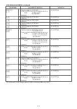
SOFTWARE ADJUSTMENT (continued)

ADJUSTMENT

ADJUSTMENT CONDITION

OPERATION

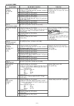
SENSITIVITY 

[      ]

1 • Operating frequency: 108.025 MHz

• Connect an SSG to the antenna connector and set as:
            Level              : –97 dBm* (3.2 µV)
                                    (No modulation)
• Receiving

• Push [ENT] key.

[      ]

2 • Operating frequency: 127.500 MHz

• Receiving

• Push [ENT] key.

[      ]

3 • Operating frequency: 136.975 MHz

• Receiving

• Push [ENT] key.

[      ]

4 • Operating frequency: 161.650 MHz

• Receiving

• Push [ENT] key.

[      ]

5 • Operating frequency: 163.275 MHz

• Receiving

• Push [ENT] key.

SQUELCH

[      ]

1 • Operating frequency: 108.025 MHz (IC-A24)

                                               118.025 MHz (IC-A6)
• Connect an SSG to the antenna connector and set as:
            Level              : –111 dBm* (0.63 µV) for IC-A24
                                    –114 dBm* (0.45 µV) for IC-A6
                                      (No modulation)
• Receiving

• Push [ENT] key.

[      ]

2 • Connect an SSG to the antenna connector and set as:

            Level              : –114 dBm* (0.45 µV) for IC-A24
                                    –117 dBm* (0.32 µV) for IC-A6
                                       (No modulation)
• Receiving

• Push [ENT] key.

[      ]

3 • Connect an SSG to the antenna connector and set as:

            Level              : –82 dBm* (18 µV) 
                                       (No modulation)
• Receiving

• Push [ENT] key.

[      ]

4 • Connect an SSG to the antenna connector and set as:

            Level              : –85 dBm* (13 µV) 
                                       (No modulation)
• Receiving

• Push [ENT] key.

[      ]

5 • Operating frequency: 162.550 MHz

• Connect an SSG to the antenna connector and set as:
            Level              : –117 dBm* (0.32 µV) 
                                       (No modulation)
• Receiving

• Push [ENT] key.

[      ]

6 • Connect an SSG to the antenna connector and set as:

            Level              : –120 dBm* (0.22 µV) 
                                       (No modulation)
• Receiving

• Push [ENT] key.

[      ]

7 • Connect an SSG to the antenna connector and set as:

            Level              : –82 dBm* (18 µV) 
                                       (No modulation)
• Receiving

• Push [ENT] key.

[      ]

8 • Connect an SSG to the antenna connector and set as:

            Level              : –85 dBm* (13 µV) 
                                       (No modulation)
• Receiving

• Push [ENT] key.

*This output level of a standard signal generator (SSG) is indicated as SSG's open circuit.

Summary of Contents for IC-A6

Page 1: ...S 14115HZ C1 q July 2007 VHF AIR BAND TRANSCEVER iC a24 iC a24e iC a6 iC a6e ...

Page 2: ...e 4 Quantity required ORDER EXAMPLE 1110003491 S IC TA31136FNG IC A24 RF UNIT 5 pieces 8820001210 Screw 2438 screw IC A24 Top cover 10 pieces Addresses are provided on the inside back cover for your convenience Icom Icom Inc and logo are registered trademarks of Icom Incorporated Japan in the United States the United Kingdom Germany France Spain Russia and or other countries ORDERING PARTS 1 Make ...

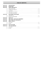
Page 3: ...SUPPLY CIRCUITS 4 4 4 5 CPU PORT ALLOCATIONS 4 5 SECTION 5 ADJUSTMENT PROCEDURES 5 1 PREPARIOTION 5 1 5 2 SOFT WEAR ADJUSTMENT 5 3 SECTION 6 PARTS LIST SECTION 7 MECHANICAL PARTS AND DISASSEMBLY SECTION 8 SEMI CONDUCTOR INFORMATION SECTION 9 BOARD LAYOUTS 9 1 LOGIC UNIT 9 1 9 2 RF UNIT 9 3 SECTION 10 BLOCK DIAGRAM SECTION 11 VOLTAGE DIAGRAMS 11 1 LOGIC UNIT 11 1 11 2 RF UNIT 11 2 ...

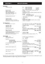
Page 4: ...ation EUR Hum and noise ratio More than 35 dB GEN USA CHN Spurious emissions More than 46 dB GEN USA CHN except operating frequency 62 5 kHz range Harmonic spurious emissions Less than 36 dBm EUR except operating frequency 1 MHz range Less than 26 dBm AUS Microphone connector impedance More than 100 kΩ 3 conductor 2 5 d mm 1 10 RECEIVER Receive system Double conversion superheterodyne Intermediate...

Page 5: ...ch IC2 TC4W53FU PLL IC IC3 TB31207AFN R5S regulator Q20 UNR9115J RX 1st mixer Q12 3SK299 RF amplifier Q11 3SK293 T5V regulater Q7 2SB1132 Q8 2SC4211 D7 MA111 2nd IF IC IC1 TA31136FN VOR switching Q19 UNR9215J IC A24 only AGC amplifier Q14 2SD1819A DC power switching Q24 HAT1024R ALC amplifier IC15 AN6123MS IC19 NJM2107F Power amplifier Q2 RD12MVS1 Antenna switches D1 D8 HVU131TRF 2 ALC attenator D...

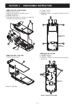
Page 6: ... 2 Remove VOL knob B and DIAL knob C 3 Unscrew the ANT nut D 4 Unscrew 3 screws E 5 Disconnect the connector F from J4 and remove the LOGIC RF unit from the Front panel REMOVING THE LOGIC UNIT 1 Remove the main seal G REMOVING THE RF UNIT 1 Unsolder 2 points K 2 Unscrew 6 screws L 3 Unscrew 2 screws M and remove the RF unit from the chassis unit 2 Unsolder 1 point H 3 Unscrew 2 nuts I 4 Unscrew 3 ...

Page 7: ...n 4 1 3 1ST MIXER AND 1ST IF CIRCUITS RF UNIT The 1st mixer circuit converts the received signal into a fixed frequency of the 1st IF signal with a PLL output frequency By changing the PLL frequency only the desired frequency will pass through a crystal filter at the next stage of the 1st mixer The signals from the RF circuit are mixed at the 1st mixer Q12 with a 1st LO signal AM 77 95 106 925 MHz...

Page 8: ...ied at the OP amplifier IC18 pins 13 14 and are then applied to the AF power amplifier IC6 pin 4 to obtain the specified audio level after being passed through the electric volume IC17 pins 21 22 The amplified AF signals are applied to the internal speaker SP1 via the SP jack J5 when no plug is connected to the jack 4 1 6 SQUELCH CIRCUIT RF AND LOGIC UNITS A squelch circuit cuts out AF signals whe...

Page 9: ...e signals to the CPU IC1 When the transceiver is set in the navigation band 108 000 117 975 MHz the VORON port of the CPU IC1 pin 118 becomes HIGH turning the VOR circuit ON via Q15 Q15 controls a 5 V power source for the VOR circuit The signal from the AM detector VORDET is buffer ampli fied at the OP AMP IC IC12 The VORDET signal includes 30 Hz variable phase com ponents and 9960 Hz reference ph...

Page 10: ...37 R24 R23 C38 From the D A converter IC16 pin 4 ALC amplifier Pre drive Q4 Q3 Q2 T5 T5 Q1 R11 VCC VCC amplifier Driver amplifier Power PWR DET LPF To the antenna D2 D3 RFDETV signal to the CPU LOGIC unit IC1 pin 30 4 2 3 DRIVE POWER AMPLIFIER CIRCUITS RF UNIT The drive amplifier circuit amplifies the transmit signal to a level needed for the power amplifier circuit The power amplifier circuit amp...

Page 11: ...e R5S regulator circuit Q20 using R5C signal from the CPU LOGIC unit IC1 The output voltage is ap plied to the RF amplifier RF unit Q12 and 1st IF amplifier RF unit Q13 etc 4 3 PLL CIRCUITS RF UNIT A PLL circuit provides stable oscillation of the transmit frequency and receive 1st LO frequency The PLL output compares the phase of the divided VCO frequency to the reference frequency The PLL output ...

Page 12: ... the battery voltage de tection 38 BEEP Outputs BEEP audio signals 109 PSTB Outputs strobe signal to the PLL IC RF unit IC3 110 PDATA Outputs data signals to the PLL IC RF unit IC3 111 PCK Outputs clock signal to the PLL IC RF unit IC3 112 TXC Outputs control signal to the T5 regu lator circuit Q7 Q8 D8 115 JACKDET Input port for external SP jack con nection detection High While external SP jack i...

Page 13: ... Turn power OFF Disconnect OPC 478 U UC from the transceiver 6 Push and hold CLR and SQL then turn power ON OPERATING ON THE ADJUSTMENT MODE Store the adjustment value ENT Change the adjustment item UP 121 5 Change the adjustment item DOWN MR Change the adjustment value DIAL EXITING THE ADJUSTMENT MODE When the adjustment is finished the transceiver must be cancelled adjustment mode to use normal ...

Page 14: ...11V BATTERY TERMINAL Standard signal generator 0 1 µV to 32 mV 127 dBm to 17 dBm CAUTION DO NOT transmit while an SSG is connected to the antenna connector To SP To MIC DC ammeter DC POWER SUPPLY 7 2 V 5 A DC ammeter PC to USB port to RS 232C port OPC 478 RS 232C type OPC 478U UC USB type PC SCREEN IN tHE ADJUSTMENT MODE CONNECTION Operating frequency Adjustment item Adjustment value DISPLAY IN TH...

Page 15: ...ET 1 Operating frequency 127 500 MHz Connect a DC ammeter between the battery terminal and DC power supply 7 2 V Measure the current at 00 point B Rotate DIAL to adjust the current B 150 mA Push ENT key 2 Operating frequency 118 025 MHz 3 Operating frequency 136 975 MHz 4 Operating frequency 127 500 MHz Connect a DC ammeter between the DC 11V jack and DC power supply 11 V 5 Operating frequency 118...

Page 16: ...75 MHz Transmitting 4 Operating frequency 127 500 MHz Connect an 11 V DC power supply to the DC 11V jack Transmitting 5 Operating frequency 118 025 MHz Transmitting 6 Operating frequency 136 975 MHz Transmitting move to MAX MODULATION for driver amp Push MR key 5 times Until you can find d7 MAX MODULATION 1 Operating frequency 127 500 MHz Connect a 7 2 V DC power supply to the battery terminal Con...

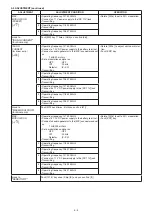
Page 17: ...enna connector and set as Level 114 dBm 0 45 µV for IC A24 117 dBm 0 32 µV for IC A6 No modulation Receiving Push ENT key 3 Connect an SSG to the antenna connector and set as Level 82 dBm 18 µV No modulation Receiving Push ENT key 4 Connect an SSG to the antenna connector and set as Level 85 dBm 13 µV No modulation Receiving Push ENT key 5 Operating frequency 162 550 MHz Connect an SSG to the ante...

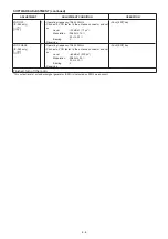
Page 18: ...l 90 dBm 7 1 µV Modulation 9960 Hz 10 30 Hz 30 Bearing 0 Receiving Push ENT key VOR PHASE IC A24 only 1 Operating frequency 108 000 MHz Connect a VOR tester to the antenna connector and set as Level 60 dBm 220 µV Modulation 9960 Hz 30 30 Hz 30 Bearing 0 Receiving Push ENT key Finished Turn off the radio This output level of a standard signal generator SSG is indicated as SSG s open circuit ...

Page 19: ...RDER DESCRIPTION M H V NO NO LOCATION R79 7030005290 S RES ERJ2GEJ 682 X 6 8 k IC A24 E only B 15 9 21 9 R80 7030005100 S RES ERJ2GEJ 154 X 150 k IC A24 E only B 13 8 20 1 R81 7030008400 S RES ERJ2GEJ 182 X 1 8 k IC A24 E only B 15 9 20 1 R82 7030005040 S RES ERJ2GEJ 472 X 4 7 k IC A24 E only B 15 20 1 R83 7030005110 S RES ERJ2GEJ 224 X 220 k IC A24 E only B 10 20 9 R84 7030005040 S RES ERJ2GEJ 47...

Page 20: ...2 C157 4030017440 S CER ECJ0EC1H221J B 55 3 27 2 C158 4030017440 S CER ECJ0EC1H221J B 56 2 27 2 C159 4030017440 S CER ECJ0EC1H221J B 58 9 27 2 C160 4030017460 S CER ECJ0EB1E102K B 52 4 33 5 C161 4030017460 S CER ECJ0EB1E102K B 60 5 7 2 C162 4030017460 S CER ECJ0EB1E102K B 63 43 C163 4030017460 S CER ECJ0EB1E102K B 63 8 30 9 C164 4030017460 S CER ECJ0EB1E102K B 60 4 40 5 C165 4030017430 S CER ECJ0E...

Page 21: ...ount RF UNIT REF ORDER DESCRIPTION M H V NO NO LOCATION D52 1790001250 S DIO MA2S111 TX T 62 9 37 5 FI1 2030000390 S MLH FL 378 30 05 MHz except AUS T 67 2 24 3 2030000610 S MLH DSF753SBFFL 4130 05MHZ AUS T 67 2 24 3 FI2 2020002160 S CER CFWKA450KFFA R0 AUS T 73 5 4 7 2020002400 S CER CFWKA450KDFA R0 except AUS T 73 5 4 7 X1 6070000191 S DCR CDBKB450KCAY24 R0 T 64 2 4 8 X2 6050012020 S XTL CR 791 ...

Page 22: ...27 R189 7030005120 S RES ERJ2GEJ 102 X 1 k B 104 9 29 5 R192 7030010010 S RES ERJ2RKF 334 X 330 k T 98 6 34 2 S Surface mount RF UNIT REF ORDER DESCRIPTION M H V NO NO LOCATION R193 7030010020 S RES ERJ2RKF 154 X 150 k T 97 3 34 R194 7030010010 S RES ERJ2RKF 334 X 330 k T 10 7 9 3 R195 7030010020 S RES ERJ2RKF 154 X 150 k T 10 7 7 2 R196 7030000160 S RES MCR10EZHJ 15 150 B 105 7 32 5 R197 70300001...

Page 23: ...95 4030016790 S CER ECJ0EB1C103K B 74 7 2 2 C96 4030016930 S CER ECJ0EB1A104K B 75 6 3 5 C97 4030016790 S CER ECJ0EB1C103K T 70 5 11 4 S Surface mount RF UNIT REF ORDER DESCRIPTION M H V NO NO LOCATION C98 4030017460 S CER ECJ0EB1E102K B 76 3 8 7 C99 4550007200 S TAN F930J476MBABMA except AUS B 106 3 5 4550007620 S TAN F931V224MAABMA AUS B 106 3 5 C100 4030016790 S CER ECJ0EB1C103K T 77 1 9 5 C101...

Page 24: ...ER ECJ0EC1H221J T 78 3 28 8 C342 4030017460 S CER ECJ0EB1E102K B 91 2 15 7 C347 4030016930 S CER ECJ0EB1A104K B 79 5 11 1 C348 4030016930 S CER ECJ0EB1A104K B 89 3 6 7 C350 4030011600 S CER C1608 JB 1E 104K T T 37 4 15 5 C351 4030009000 S CER C2012 JB 1C 224K T B 49 6 10 7 C352 4030018890 S CER ECJ0EB0J224K B 52 9 10 5 C354 4030012600 S CER C2012 JB 1A 105M T B 88 9 11 9 C355 4030012600 S CER C201...

Page 25: ... W except A24E A6E 2 MP31 8930065090 2791 PET SHEET 1 MP32 8930065140 2791 MIC SPONGE 1 MP33 8860001350 2791 EARTH PLATE 1 MP35 8810009561 Screw BT B0 2X6 NI ZK3 BT 2 MP36 8810009511 Screw BT B0 2X4 NI ZC3 BT 13 MP37 8810004861 Screw PH M2X6 ZK3 2 MP38 8810009181 0tap 1flat washer B0 2X5 NI ZC3 BT 1 MP39 8810010191 Screw BiH M2X4 SUS SSBC 1 MP41 8930065490 RUBBER SHEET BO 1 MP42 8510017010 2791 SH...

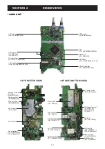
Page 26: ... C MP5 C MP1 C MP25 C MP26 C SP1 C W1 C MP16 C MP3 C MP4 C MP12 C MP11 C MP23 C MP19 C MP20 C MP1 R S1 R J2 R J5 R J1 R S2 R MP37 C MP2 C MP33 C MP13 C MP15 C MP24 C MP22 C MP36 C MP35 C MP38 C MP14 C J1 C Note C CHASSIS PARTS R RF UNIT L LOGIC UNIT LOGIC UNIT RF UNIT 54 21 8 128 9 5 1 16 144 9 5 23 32 0 4 1 32 5 6 7 32 2 8 1 8 35 5 13 32 39 5 9 16 333 8 13 5 32 0 4 1 32 17 9 23 32 Unit mm inch ...

Page 27: ...D2 D2 D1 D1 G2 S2 G1 S1 D S G2 G1 B E C B E C B E C B E C B E C E1 C2 B1 C1 E2 B2 E1 C2 B1 C1 E2 B2 B1 E B2 C1 C2 B1 E B2 C1 C2 E1 B1 B2 C1 C2 2SA1586 GR 2SA1588 GR 2SB1132 T100 R 2SB1182 TL Q 2SB1201 S 2SC3357 T1 RF 2SC4116 BL 2SC4211 6 TL 2SC4215 O 2SC4226 T1 R25 2SC4403 3 TL 2SC4617 TLS 2SD1819 A R 2SK880 Y 3SK293 3SK299 T1 U73 HAT1024R RD01MUS1 RD12MVS1 T12 UNR9110J UNR9115J UNR9210J UNR9211J ...

Page 28: ...OUTS LOGIC UNIT TOP VIEW PWR F CLR ANL 121 5 3 2 1 6 5 4 9 8 7 MR 0 ENT SQL DS2 DS3 DS5 DS6 DS7 DS8 DS9 DS10 MC1 H0 H5 H10 H15 H20 H25 H30 H35 H40 H45 H50 H55 H60 H65 H70 H75 H80 H85 H90 V0 V5 V10 V15 V20 V25 V30 V35 V40 V45 ...

Page 29: ...C170 C171 C172 C173 C174 C175 C176 C177 C178 C179 C180 C181 C182 C183 C184 C600 C602 C603 C604 C605 C606 C607 C608 C609 C610 C611 C612 C613 C614 C615 C616 C617 C618 C619 C620 C621 C622 C623 D1 D2 D5 D6 D7 D8 D10 D11 D16 D17 D18 D19 IC1 IC2 IC3 IC7 IC11 IC12 IC13 IC14 IC16 J1 J1 Q1 Q2 Q3 Q4 Q5 Q6 Q7 Q8 Q9 Q13 Q15 Q16 R1 R2 R5 R11 R12 R13 R14 R15 R16 R17 R18 R20 R21 R22 R25 R26 R30 R36 R60 R61 R62 R...

Page 30: ... C311 C312 C313 C315 C316 C317 C318 C319 C330 C331 C335 C336 C337 C338 C339 C340 C350 C362 C363 C384 C385 C387 C410 C412 C413 C415 C417 C429 C430 CP4 D1 D4 D5 D6 D8 D30 D31 D37 D38 D39 D42 D45 D46 D47 D48 D51 D52 EP2 EP4 EP13 EP14 EP16 FI1 FI2 IC15 IC16 IC18 IC19 J1 J2 J4 J5 J6 L1 L2 L3 L5 L6 L7 L8 L10 L11 L12 L13 L14 L15 L16 L44 L45 L46 L55 L56 L57 L58 L59 L60 L63 L64 L67 L71 L72 L78 MP3 Q2 Q3 Q4...

Page 31: ...22 D23 D27 D29 D32 D36 D40 D41 D43 D44 EP3 EP5 EP6 EP7 EP8 EP10 EP11 EP15 IC1 IC2 IC3 IC5 IC6 IC13 IC17 L4 L17 L18 L21 L22 L23 L24 L38 L42 L50 L51 L52 L68 L70 L73 L74 L75 L80 L81 L82 L83 L84 L85 L86 MP1 MP2 Q1 Q7 Q8 Q9 Q10 Q11 Q12 Q14 Q15 Q16 Q17 Q18 Q19 Q20 Q21 Q24 Q25 Q26 Q28 Q29 Q39 Q40 Q41 Q45 Q50 Q51 Q61 R2 R3 R4 R5 R6 R7 R8 R9 R10 R11 R12 R13 R23 R40 R41 R42 R43 R44 R45 R46 R47 R48 R49 R51 R...

Page 32: ...4 4 Q57 XP1113 Q33 2SC4116 D1 D8 D9 HVU131TRF 3 T5 D29 1SV271 Q9 2SD1819A D13 MA2S304 Q10 2SD1819A Q11 3SK293 D14 D16 D44 D43 MA2S077 MA2S304 4 Q12 3SK299 Q13 2SC4215 29 6MHz IC3 TB31207AFN Q45 2SK880 REG Q7 2SB1132 Q8 2SC4211 D7 MA111 R5S IC1 TA31136FN Q15 2SC4215 Q16 2SC4215 Q17 2SC4215 D40 1SV271 D41 1SV271 Q18 Q21 UNR9210J Q19 UNR9215J D18 MA785 IC2 TC4W53FU REG T5 R5S IC13 NJM2107F Q20 UNR911...

Page 33: ...1 S10 62 S11 63 S12 64 S13 65 S14 66 S15 67 S16 68 S17 69 S18 70 S19 71 S20 72 S21 73 S22 74 S23 75 P90 S24 76 P91 S25 77 P92 S26 78 P93 S27 79 P94 S28 80 P95 S29 81 P96 S30 82 P97 S31 83 P80 S32 84 P81 S33 85 P82 S34 86 P83 S35 87 P84 S26 88 P85 S37 89 P86 S38 90 P87 S39 91 VSS0 92 VDD0 93 P60 94 P61 95 P62 96 P63 97 P64 98 P65 99 P66 100 P67 101 P40 102 P41 103 P42 104 P43 105 P44 106 P45 107 P4...

Page 34: ...0 R212 47K 1 5P C317 0 001 C46 10U L57 47K R242 MPZ2012S331A EP7 MA2S111 D32 0 001 C101 MA77 D6 0 001 C278 0 001 C84 0 1 C96 0 001 C309 68 R337 0 01 C100 Q33 2SC4116 L38 0 27U 82P C398 150P C368 R133 22K NTCG16 R328 SP1 0 1 C259 0 001 C87 ACZ1005Y EP14 2SC4211 Q18 0 001 C20 0 001 C263 R30 10 R24 22K 0 001 C172 0 001 C410 0 001 C44 R47 100K R149 10K 0 001 C279 L51 100U 22K R258 0 15U L82 0 001 C93 ...

Page 35: ...Glenwood Centre 150 6165 Highway 17 Delta B C V4K 5B8 Canada Phone 1 604 952 4266 Fax 1 604 952 0090 URL http www icomcanada com E mail info icomcanada com Unit 1 103 Garden Road Clayton VIC 3168 Australia Phone 61 03 9549 7500 Fax 61 03 9549 7505 URL http www icom net au E mail sales icom net au 146A Harris Road East Tamaki Auckland New Zealand Phone 64 09 274 4062 Fax 64 09 274 4708 URL http www...

Page 36: ...1 1 32 Kamiminami Hirano ku Osaka 547 0003 Japan S 14115HZ C1 q 2004 2007 Icom Inc ...

Reviews: