background image


65

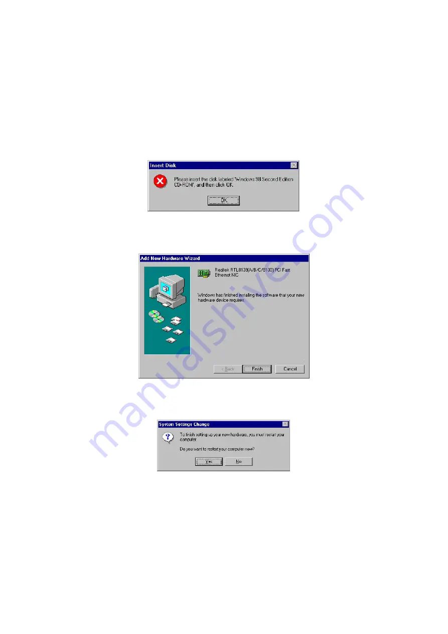
11. When copying of driver files finishes, the program will then ask 

you to insert your Windows.  


12. The program then copies the necessary files from your Windows 

installation disk to complete the driver setup process. Once the 
driver is completely installed, the following message appears on 
your display. Click on the Finish button to proceed. 


13. Restart your computer to make the new system settings take 

effect. Click on the Yes button when the screen below appears 
and your LAN Driver for Win95 and Win98 are now completely 
installed. 


Summary of Contents for HS-2608

Page 1: ... Celeron Processor Embedded Engine Board CompactFlash Mini PCI SO DIMM CRT LVDS Panel Dual LAN Audio ATA 33 66 100 RS 232 422 485 4 COM USB PC 104 DOC WDT Single 5V H W Monitor Industrial Embedded Single Board computer ...

Page 2: ...ranted permission by BOSER Technology Co Ltd BOSER Technology Co Ltd reserves the right to change or improve the contents of this document without due notice BOSER Technology Co Ltd assumes no responsibility for any errors or omissions that may appear in this manual nor does it make any commitment to update the information contained herein T T Tr r ra a ad d de e em m ma a ar r rk k ks s s BOSER i...

Page 3: ...6 System Memory 10 3 7 DiskOnChip Address Setting 10 3 8 VGA Controller 12 3 9 PCI E IDE Drive Connector 14 3 10 Floppy Disk Drive Connector 15 3 11 Serial Port Connectors 16 3 12 Parallel Connector 19 3 13 Ethernet Connector 20 3 14 USB Connector 20 3 15 CMOS Data Clear 21 3 16 Power and Fan Connectors 21 3 17 Keyboard Mouse Connectors 22 3 18 System Front Panel Connectors 22 3 19 Watchdog Timer ...

Page 4: ...eripheral Setup 41 4 10 Hardware Monitor Setup 42 4 11 Auto Detect Hard Disks 42 4 12 Change Supervisor User Password 43 4 13 Auto Configuration with Optimal Settings 44 4 14 Auto Configuration with Fail Safe Settings 45 4 15 Save Settings and Exit 46 4 16 Exit Without Saving 47 Chapter 5 Software Utilities 49 5 1 IDE Driver Installation 49 5 2 VGA Driver Installation 54 5 3 LAN Driver Installatio...

Page 5: ... strap available from most electronic component stores when handling boards and components Fasten the ALLIGATOR clip of the strap to the end of the shielded wire lead from a grounded object Please wear and connect the strap before handle the HS 2608 to ensure harmlessly discharge any static electricity through the strap Please use an anti static pad when putting down any components or parts or too...

Page 6: ......

Page 7: ...ransfers of 33 66 or 100MB sec to one IDE drive connection Designed with the VIA VT8606 core logic chipset the board supports ULV Intel Celeron processor 400MHz 650MHz The VIA VT8606 with 32MB shared main memory supporting CRT Panel displays up to 1280 x 1024 at 24bpp colors CRT 1024 x 768 at 18bpp colors Panel It also supports 18 bit dual channel LVDS interface System memory is also sufficient wi...

Page 8: ...uch condition 1 1 Major Features The HS 2608 v2 0 comes with the following features ULV Intel Celeron processor 400MHz 650MHz One SO DIMM socket with a max capacity of 512MB VIA VT8606 VT82C686B system chipset VIA VT82C686B SMC 37C669 super I O chipset VIA VT8606 graphics controller 18 bit 36 bit LVDS Panel display interface Dual RealTek RTL8139DL LAN controller AC97 3D audio controller Fast PCI A...

Page 9: ... RTL8139DL 10 100 Based LAN Audio AC97 3D audio controller IDE One 2 0 pitch 44 pin IDE connector FDD Supports up to two floppy disk drives Parallel One enhanced bi directional parallel port supporting SPP ECP EPP Serial Port 16C550 UART compatible RS 232 422 485 x 1 and RS 232 x 3 serial ports with 16 byte FIFO USB 2 internal USB ports PC 104 PC 104 Bus connector for 16 bit ISA Bus Keyboard Mouse...

Page 10: ...4 1 3 Board Dimensions ...

Page 11: ...ed surface and carefully inspect the board for any damage that might have occurred during shipment Ground the board and exercise extreme care to prevent damage to the board from static electricity Integrated circuits will sometimes come out of their sockets during shipment Examine all integrated circuits particularly the BIOS processor memory modules ROM Disk and keyboard controller chip to ensure...

Page 12: ...u want to use ATA 66 100 IDE device please purchase this cable separately Optional Cable Part No Description 291 04010200G ATA 66 100 IDE cable for 2 0 pitch IDE connector It is recommended that you keep all the parts of the delivery package intact and store them in a safe dry place for any unforeseen event requiring the return shipment of the product In case you discover any missing and or damage...

Page 13: ...owing are important reminders and steps to take before you begin with your installation process 1 Make sure that all jumper settings match their default settings and CMOS setup correctly Refer to the sections on this chapter for the default settings of each jumper 2 Go through the connections of all external devices and make sure that they are installed properly and configured correctly within the...

Page 14: ...8 3 2 Board Layout ...

Page 15: ...er In Connector 21 CN3 CN4 PC 104 40 pin 64 pin Connector 26 CN5 2 pin Power In Connector 21 CN6 8 bit I O Connector 29 CN8 Floppy Connector 15 CN9 Line In Audio Out Connector 28 CN10 RS 422 485 Connector 2x3 header 16 CN12 Parallel Connector 19 CN13 CN28 RJ 45 Connector 20 CN16 CN18 CN14 CN19 COM 1 COM 4 Connector 5x2 header 16 CN15 PS 2 6 pin Mini DIN KB MS Connector 22 CN17 6 pin KB MS Connecto...

Page 16: ...hip module socket Jumper JP4 1 4 assigns the starting memory address of the installed module If you have another memory device that has a similar memory capacity with that of the DOC in your system please set both at different memory address mapping to avoid the mapping area conflicts Failing to do so will not make the HS 2608 v2 0 and the additional memory device function properly JP4 1 4 DiskOnC...

Page 17: ...u encounter difficulty installing your DiskOnChip module please consult a qualified technician or engineer to perform the installation 3 7 2 Removing DiskOnChip Modules When removing a DiskOnChip module from its socket please take note of the following 1 Loosen the contact of the module from its socket using a screwdriver 2 Insert the screwdriver s flat head into a gap on either end of the socket ...

Page 18: ...D 7 GND 8 GND 9 N C 10 GND 11 N C 12 SDA 13 HSYNC 14 VSYNC 15 SCL 1 6 10 11 5 15 CN26 CN27 LVDS Interface Connector PIN Description PIN Description 1 VLCD 2 VLCD 3 Y0M Z0M 4 Y0P Z0P 5 Y1M Z1M 6 Y1P Z1P 7 Y2M Z2M 8 Y2P Z2P 9 Y3M Z3M 10 Y3P Z3P 11 GND 12 GND 1 2 12 11 VLCD Y0 Y2 Y4 Y6 GND VLCD Y1 Y3 Y5 Y7 GND NOTE LVDS cable should be produced very carefully Y0 Y1 have to be fabricated in twister pa...

Page 19: ... P33 49 P34 50 P35 1 2 50 49 N C GND 3 3V 5V ENAVEE PD0 PD2 PD4 PD6 PD8 PD10 PD12 PD14 PD16 PD18 PD20 N C GND ENAVDD GND PD1 PD3 PD5 PD7 PD9 PD11 PD13 PD15 PD17 PD19 PD21 PD22 PD24 SHFCLK DE GND P26 P28 P30 P32 P34 PD23 PD25 FLM LP ENABKL P27 P29 P31 P33 P35 NOTE Please set the proper voltage of your panel using JP7 before proceeding on installing it The HS 2608 v2 0 has an onboard jumper that sel...

Page 20: ... 8 PDD10 9 PDD4 10 PDD11 11 PDD3 12 PDD12 13 PDD2 14 PDD13 15 PDD1 16 PDD14 17 PDD0 18 PDD15 19 GND 20 N C 21 PDDREQ 22 GND 23 IOW 24 GND 25 IOR 26 GND 27 PIORDY 28 470Ω with GND 29 PDDACK 30 GND 31 IRQ14 32 N C 33 PDA1 34 PD33 66 35 PDA0 36 PDA2 37 PDCS1 38 PDCS3 39 HDD Active 40 GND 41 VCC 42 VCC 43 GND 44 N C IDERST PDD7 PDD6 PDD5 PDD4 PDD0 GND PDDREQ IOW IOR PIORDY PDDACK IRQ14 PDA1 PDD3 PDD2 ...

Page 21: ...ard 34 pin header connector CN8 for floppy disk drive connection A total of two FDD drives may be connected to CN8 at any given time CN8 Floppy Connector PIN Description PIN Description 1 GND 2 DRVDEN0 3 GND 4 N C 5 GND 6 DRVDEN1 7 GND 8 INDEX 9 GND 10 MTR0 11 GND 12 DS1 13 GND 14 DS0 15 GND 16 MTR1 17 GND 18 DIR 19 GND 20 STEP 21 GND 22 WDATA 23 GND 24 WGATE 25 GND 26 TRAK00 27 GND 28 WRTPRT 29 G...

Page 22: ...6 byte FIFO serial ports and four internal 10 pin headers and one RS 422 485 connector CN16 COM1 Connector 5x2 Header PIN Description PIN Description 1 DCD1 2 DSR1 3 RXD1 4 RTS1 5 TXD1 6 CTS1 7 DTR1 8 RI1 9 GND 10 N C 2 4 6 8 10 1 3 5 7 9 DSR1 RTS1 CTS1 N C RI1 DCD1 RXD1 TXD1 GND DTR1 CN18 COM2 Connector 5x2 Header PIN Description PIN Description 1 DCD2 2 DSR2 3 RXD2 4 RTS2 5 TXD2 6 CTS2 7 DTR2 8 ...

Page 23: ...RTS4 CTS4 N C RI4 DCD4 RXD4 TXD4 GND DTR4 CN10 RS 422 485 Connector 5x2 Header COM2 PIN Description PIN Description 1 TX 2 TX 3 RX 4 RX 5 GND 6 RTS 2 4 6 1 3 5 TX RX VCC TX RX GND NOTE The terminal resistance of RX TX is set at 180Ω JP5 JP6 RS 232 422 485 Function Enabled Disabled Select Settings Options JP5 7 8 JP6 RS 232 default Open Open RS 485 by Auto 1 2 3 5 6 8 Short Short RS 485 by RTS 1 2 ...

Page 24: ...18 RS 422 for 4 wires Typical RS 485 2 wires Multidrop Network Typical RS 485 4 wires Multidrop Network ...

Page 25: ...DATA 0 15 ERROR 3 DATA 1 16 Initialize 4 DATA 2 17 Printer Select LN 5 DATA 3 18 GND 6 DATA 4 19 GND 7 DATA 5 20 GND 8 DATA 6 21 GND 9 DATA 7 22 GND 10 Acknowledge 23 GND 11 Busy 24 GND 12 Paper Empty 25 GND 13 Printer Select 26 GND 1 14 26 13 Auto Form Feed ERROR Initialize Printer Select LN GND GND GND GND GND GND GND GND GND Strobe DATA0 DATA1 DATA2 DATA3 DATA4 DATA5 DATA6 DATA7 Acknowledge Bus...

Page 26: ...1 TX 2 TX 3 RX 4 R C GND 5 R C GND 6 RX 7 R C GND 8 R C GND 8 4 2 1 R C GND RX R C GND TX R C GND R C GND RX TX 3 14 USB Connector The HS 2608 v2 0 provides one 8 pin connectors at location CN1 for two USB connections to the HS 2608 v2 0 CN1 USB Connector PIN Description PIN Description 1 VCC 2 VCC 3 USBD1 4 USBD0 5 USBD1 6 USBD0 7 GND 8 GND 1 2 7 8 VCC USBD0 USBD0 GND VCC USBD1 USBD1 GND ...

Page 27: ...wer and Fan Connectors HS 2608 v2 0 provides one 5 pin power connectors at CN2 And one 2 pin power in at CN5 CN2 5 pin ATX Power In Connector PIN Description PIN Description 1 GND 2 PS_ON 3 12V 4 5VSB 5 VCC 1 GND 5 PS_ON 12V 5VSB VCC CN5 2 pin Power In Connector PIN Description 1 VCC 2 GND 1 VCC 2 GND FN1 Fan Connector PIN Description 1 CPU Fan1 2 5V 3 GND 1 GND 3 5V Fan Speed Connector FN1 onboar...

Page 28: ...ta Mouse Data GND 5V 1 2 3 4 5 6 Keyboard Clock Mouse Clock CN17 6 pin Keyboard Mouse Connector PIN Description 1 Keyboard Clock 2 Keyboard Data 3 Mouse Data 4 GND 5 5V 6 Mouse Clock Keyboard Clock Keyboard Data Mouse Data GND 1 2 3 4 5 6 5V Mouse Clock 3 18 System Front Panel Connectors The HS 2608 v2 0 has one LED at location JP3 that indicates the power on status This visual feature of the IDE ...

Page 29: ...imer There are three access cycles of Watch Dog Timer as Enable Refresh and Disable The Enable cycle proceeds via READ PORT 443H whereas the Disable cycle proceeds via READ PORT 045H A continued Enable cycle after a first Enable cycle means Refresh Once the Enable cycle is active a Refresh cycle is requested before the time out period This restarts counting of the WDT period When the time counting...

Page 30: ...via a Disable cycle and reading the disable control port 045H After an Enable cycle of WDT user must immediately execute a Refresh cycle to WDT before its period setting comes to an end every 1 2 10 20 110 or 220 seconds If the Refresh cycle does not activate before WDT period cycle the onboard WDT architecture will issue a Reset or NMI cycle to the system There are three I O ports that control th...

Page 31: ... PUSH AX PUSH DX MOV DX WDT_DIS disable the WDT IN AL DX POP DX get back AX DX POP AX RET 3 20 Mini PCI Connector HS 2608 v2 0 supports a Mini PCI connector at PC1 The peripheral component with standard Type1 Mini PCI can be used For particular requirement please refer to BOSER Mini PCI series product on website or contact with us ...

Page 32: ...tables NOTE The PC 104 connector allows direct plugging or stack through piling of PC 104 modules without requiring the PC 104 mounting kit CN3 PC 104 40 pin Connector PIN Description PIN Description 1 GND 21 GND 2 MEMCS16 22 SBHE 3 IOSC16 23 SA23 4 IRQ10 24 SA22 5 IRQ11 25 SA21 6 IRQ12 26 SA20 7 IRQ15 27 SA19 8 IRQ14 28 SA18 9 DACK0 29 SA17 10 DRQ0 30 MEMR 11 DACK5 31 MEMW 12 DRQ5 32 SD8 13 DACK6...

Page 33: ... 43 SMEMW 12 SA19 44 SMEMR 13 SA18 45 IOW 14 SA17 46 IOR 15 SA16 47 DACK3 16 SA15 48 DRQ3 17 SA14 49 DACK1 18 SA13 50 DRQ1 19 SA12 51 REFRESH 20 SA11 52 SYSCLK 21 SA10 53 IRQ7 22 SA9 54 IRQ6 23 SA8 55 IRQ5 24 SA7 56 IRQ4 25 SA6 57 IRQ3 26 SA5 58 DACK2 27 SA4 59 TC 28 SA3 60 BALE 29 SA2 61 5V 30 SA1 62 OSC 31 SA0 63 N C 32 GND 64 GND Connector diagram rotated 90 degrees clockwise from original posi...

Page 34: ...ector which is IDE interface located at the solder side of the board beneath the SO DIMM connector The designated CN24 connector once soldered with an adapter can hold CompactFlash cards of various sizes Please turn off the power before inserting the CD card CN24 CompactFlash Connector PIN Description PIN Description 1 GND 2 DATA 3 3 DATA 4 4 DATA 5 5 DATA 6 6 DATA 7 7 SDCS1 8 GND 9 GND 10 GND 11 ...

Page 35: ...e diagram on the following page for the traditional way of inserting the card C o m p a c t F la s h T M C EM a d e in J a p a n F a b ri q u e A u J a p o n C F R e a r S id e P C B S o l d e r S i d e V i e w 3 24 8 bit I O Function The HS 2608 v2 0 offers one 8 bit input output port by parallel port CN6 8 bit Input Output PIN Description PIN Description 1 VCC 2 GND 3 GD0 4 GD4 5 GD1 6 GD5 7 GD2...

Page 36: ... near mov ax data mov ds ax STI Mov dx port Mov al 80h out dx al ROR mov cx 08h ror al 1 call delay out dx al loop b pop cx ROL push cx mov cx 08h rol al 1 out dx al call delay loop b pop cx ROR mov cx 08h ror al 1 call delay out dx al loop b pop cx ROL push cx mov cx 08h rol al 1 out dx al call delay loop b pop cx ...

Page 37: ... dx al call delay loop b pop cx ROR mov cx 08h ror al 1 call delay out dx al loop b pop cx ROL push cx mov cx 08h rol al 1 out dx al call delay loop b pop cx ROR mov cx 08h ror al 1 call delay out dx al loop b pop cx ROL push cx mov cx 08h rol al 1 out dx al call delay loop b pop cx ROR mov cx 08h ...

Page 38: ...loop b pop cx ROR mov cx 08h ror al 1 call delay out dx al loop b pop cx ROL push cx mov cx 08h rol al 1 out dx al call delay loop b pop cx flash LED 3 time mov cx 01h mov al 0ffh out dx al call delay mov al 0h out dx al call delay loop b ee mov ah 4ch go back to dos int 21h stack begin endp end begin ...

Page 39: ... on one of the disks and then launch and turn control over to the operating system While the BIOS is in control the Setup program can be activated in one of two ways 1 By pressing Del immediately after switching the system on or 2 By pressing the Del key when the following message appears briefly at the bottom of the screen during the POST Power On Self Test Press DEL to enter SETUP If the message...

Page 40: ...not save changes into CMOS Status Page Setup Menu and Option Page Setup Menu Exit current page and return to Main Menu PgUp key Decrease the numeric value or make changes PgDn key Increase the numeric value or make changes key Increase the numeric value or make changes key Decrease the numeric value or make changes F1 key Reserved F2 key Change color from total 8 colors F2 to select color forward ...

Page 41: ...Rights Reserved Standard CMOS Setup Advanced CMOS Setup Advanced Chipset Setup Power Management Setup PCI Plug and Play Setup Peripheral Setup Hardware Monitor Setup Auto Detect Hard Disks Change User Password Change Supervisor Password Auto Configuration with Optimal Settings Auto Configuration with Fail Safe Settings Save Settings and Exit Exit Without Saving Standard CMOS setup for changing tim...

Page 42: ...lity in BIOS SETUP to install the HDD correctly AMIBIOS SETUP STANDARD CMOS SETUP C 2001 American Megatrends Inc All Rights Reserved Date mm dd yyyy Thu Apr 17 2003 Base Memory 639KB Time hh mm ss 19 04 12 Extd Memory 55MB Floppy Drive A 1 44MB 3 1 2 Floppy Drive B Not Installed LBA Blk PIO 32Bit Type Size Cyln Head WPcom Sec Mode Mode Mode Mode Pri Master Auto ON Pri Slave Auto ON Sec Master Auto...

Page 43: ...t Boot Device Floppy 2nd Boot Device IDE 0 3rd Boot Device CD ROM Try Other Boot Devices Yes Init Display Mode Silent Display Mode at Add on ROM Init Force BIOS S M A R T for Hard Disks Disabled BootUp Num Lock On Floppy Drive Swap Disabled Floppy Drive Seek Disabled PS 2 Mouse Support Enabled Primary Display VGA EGA Password Check Setup Boot To OS 2 No Wait For F1 If Error Enabled CPU MicroCode U...

Page 44: ...ou discover that the data has been lost while using your system AMIBIOS SETUP ADVANCED CHIPSET SETUP C 2001 American Megatrends Inc All Rights Reserved DRAM Timing Available Options Configure SDRAM Timing by SPD Disabled Disabled DRAM Frequency 100Mhz Enabled SDRAM CAS Latency 3 DRAM Bank Interleave Enabled Memory Hole Disabled AGP Mode 4x AGP Fast Write Disabled AGP Comp Driving Auto Manual AGP C...

Page 45: ...pend Time Out Minute Disabled Throttle Slow Clock Ratio 50 56 25 Display Activity Ignore IRQ3 Monitor IRQ4 Monitor IRQ5 Ignore IRQ7 Monitor IRQ9 Ignore IRQ10 Ignore IRQ11 Ignore IRQ12 Ignore IRQ13 Ignore IRQ14 Monitor IRQ15 Ignore System Thermal Disabled Thermal Active Temperature 65 C 149 F Thermal Slow Clock Ratio 50 56 25 Power Button Function On Off Restore on AC Power Loss Last State Resume O...

Page 46: ...merican Megatrends Inc All Rights Reserved Plug and Play Aware O S No Available Options Clear NVRAM No No OnChip VGA Frame Buffer Size 8MB Yes PCI Latency Timer PCI Clocks 32 Primary Graphics Adapter PCI Boot Screen Select Both CRT LCD LCD Panel Type 0 640 x 480 TFT PCI IDE Bus Master Enabled OffBoard PCI IDE Card Auto OffBoard PCI IDE Primary IRQ Disabled OffBoard PCI IDE Secondary IRQ Disabled D...

Page 47: ...e complete task by them This is much simpler and more efficient also faster AMIBIOS SETUP PERIPHERAL SETUP C 2001 American Megatrends Inc All Rights Reserved OnBoard FDC Enabled Available Options OnBoard Serial Port 1 3F8 COM1 Auto OnBoard Serial Port 2 2F8 COM2 Disabled Serial Port2 Mode Normal Enabled Duplex Mode N A OnBoard Prarllel Port 378 Parallel Port Mode ECP EPP Version N A Parallel Port ...

Page 48: ...g in sequence inside a box To accept the displayed entries press the Y key to skip to the next drive press the N key If you accept the values the parameters will appear listed beside the drive letter on the screen AMIBIOS HIFLEX SETUP UTILITY VERSION x xx C 2001 American Megatrends Inc All Rights Reserved Standard CMOS Setup Advanced CMOS Setup Advanced Chipset Setup Power Management Setup PCI Plu...

Page 49: ...e the options of the setup menus user password just can only enter but do not have the right to change the options of the setup menus When you select this function the following message will appear at the center of the screen to assist you in creating a password ENTER PASSWORD Type the password up to eight characters in length and press Enter The password typed now will clear any previously entere...

Page 50: ... Setup prompting only occurs when trying to enter Setup 4 13 Auto Configuration with Optimal Settings When you press Enter on this item you will get a confirmation dialog box with a message shown below This option allows you to load restore the BIOS default values permanently stored in the BIOS ROM Pressing Y loads the BIOS default values for the most stable AMIBIOS HIFLEX SETUP UTILITY VERSION x ...

Page 51: ...he default values that are factory settings for optimal performance system operations AMIBIOS HIFLEX SETUP UTILITY VERSION x xx C 2001 American Megatrends Inc All Rights Reserved Standard CMOS Setup Advanced CMOS Setup Advanced Chipset Setup Power Management Setup Load failsafe settings Y N N Change Supervisor Password Auto Configuration with Optimal Settings Auto Configuration with Fail Safe Sett...

Page 52: ...ord Auto Configuration with Optimal Settings Auto Configuration with Fail Safe Settings Save Settings and Exit Exit Without Saving Write the current setting to CMOS and exit ESC Exit Sel F2 F3 Color F10 Save Exit Pressing Y stores the selections made in the menus in CMOS a special section of memory that stays on after you turn your system off The next time you boot your computer the BIOS configure...

Page 53: ... AMIBIOS HIFLEX SETUP UTILITY VERSION x xx C 2001 American Megatrends Inc All Rights Reserved Standard CMOS Setup Advanced CMOS Setup Advanced Chipset Setup Power Management Setup Quit without saving Y N N Change Supervisor Password Auto Configuration with Optimal Settings Auto Configuration with Fail Safe Settings Save Settings and Exit Exit Without Saving Exit without saving the current setting ...

Page 54: ...48 This page is intentionally left blank ...

Page 55: ...5 1 IDE Driver Installation The utility disk that came with the delivery package contains an auto run program that invokes the installation programs for the IDE VGA and Audio drivers The following describes the installation procedures of each driver 1 Insert Utility CD Disk to your CD ROM The main menu will pop up as shown below ...

Page 56: ...50 2 Press VIA 4 IN 1 and to go Setup 3 Once the Welcome screen appears on the screen make sure to close any applications running and then click on the Next button ...

Page 57: ...s on the screen you may read the whole document including the license agreement or just press Yes to skip through and continue installation 5 The 4 in 1 Setup dialog is now displayed Select on Normally Install and then click on Next ...

Page 58: ...en proceed by clicking on the Next button below the screen 7 The program starts to install the ATAPI driver when you click the Next button on the screen below 8 When the ATAPI driver is completely installed The utility then displays your DMA mode status and allows you to enable it Tick on the box and press on the Next button to continue ...

Page 59: ...ing the AGP driver in standard o turbo mode Select on the Standard Mode and then click on Next to proceed 10 Installation of the AGP driver is now complete Once the screen below appears select on restarting your computer to activate all drivers settings completed ...

Page 60: ...tion for WIN95 98 2K 1 With the Utility CD Disk still in your CD ROM drive open the File Manager and then select the CD ROM drive As soon as the system reads the disk the VGA Menu screen below will appear on your display Click on VIA_8606 from the main menu ...

Page 61: ...55 2 Select the operating system of your computer to proceed with the installation process ...

Page 62: ...een make sure to close applications that are running and then click the Next button 4 When the display below appears on your screen Setup is already ready to install and copy the related files onto your hard drive Click on the Next button to proceed ...

Page 63: ...on the Finish button to reboot 5 2 2 VGA Driver Installation for WIN NT4 0 1 Click the Start button on the lower left hand corner of your screen then select Setting Choose Control Panel and double click on the Display icon to launch its Display Properties window Click on the Settings tab and then choose Display Type In the Change Display Type window click on Have Disk ...

Page 64: ...58 2 Specify the path of the new driver and then press on Enter If in driver D type d Vga Via_8606 Nt40 3 Select S3 Graphics Twister 6 Click OK or press Enter ...

Page 65: ... You will see warning panel about Third Party Drivers Click on Yes to finish the installation 8 Once the installation is completed you must shut down the system and restart for the new driver to take effect ...

Page 66: ... 1 LAN Driver Installation for WIN95 98 2K 1 With the Utility CD Disk still in your CD ROM drive right click on My Computer icon from the Windows menu Select on System Properties and then proceed to the Device Manager from the main menu ...

Page 67: ...61 2 Select on Other Devices from the list of devices then double click on PCI Ethernet Controller ...

Page 68: ...ect Driver from the main menu to proceed 4 The window then displays the current status of your LAN driver Press on Update Driver button to continue 5 The program will then launch the Update Device Driver Wizard window that will install your device driver Click on the Next button to proceed to the next step ...

Page 69: ...better driver Click on the Next button to proceed 7 The Update Device Driver Wizard will then ask you to specify by ticking the path of the new driver Tick on the open boxes where you require the program to search for the device driver then click on the Browse button to manually specify the path ...

Page 70: ... 9 Once the program returns to the Add New Hardware Wizard screen your specified location will appear Press on the Next button to continue 10 Once the program detects the device driver inf file from your specified location it will automatically copy the files into your hard drive ...

Page 71: ...tallation disk to complete the driver setup process Once the driver is completely installed the following message appears on your display Click on the Finish button to proceed 13 Restart your computer to make the new system settings take effect Click on the Yes button when the screen below appears and your LAN Driver for Win95 and Win98 are now completely installed ...

Page 72: ...ith the Utility CD Disk still in your CD ROM drive right click on Network Neighborhood icon from the Windows menu Select on Properties 2 The system automatically detects the absence of Windows NT Networking Click on the Yes button to start installation ...

Page 73: ...67 3 Tick on the Wired to Network once the following screen appears Click on the Next to proceed 4 Click on the Start Search button for the program to locate the Network Adapter ...

Page 74: ...l list a number of adapters for you to choose from Press on the Have Disk button to assign the driver path location 6 Setup now asks you for the location of the driver When you have entered the new driver path press on the OK button to continue ...

Page 75: ...eds about the new driver it will display the device it found on the following screen Press on the OK button to accept and proceed 8 Setup then returns to Network Setup Wizard screen and displays your new Network Adapter Click on Next to continue ...

Page 76: ...elect the appropriate protocol and then click on Next to continue 10 Before Setup starts installing the components found and the settings you made it will give you the option to proceed or go back for changes from the following screen Click on the Next button once you are sure of your devices ...

Page 77: ...es necessary to update the system information Specify the path then press Continue 12 Once it finishes copying the files Setup will now allow you to choose the Duplex Mode of your LAN controller Press on the Continue button after making your selection ...

Page 78: ...72 13 When Setup asks if you wish to change the TCP IP settings of your system select the appropriately The default choice is No 14 Setup then starts the Networking installation and copies the files ...

Page 79: ...ishes copying the TCP IP properties of your system will then pop up on your screen like the one shown below Make the necessary changes then click on OK to continue 16 When the screen below appears click on Next to continue ...

Page 80: ...p then prompts you that it is ready to start the network You may complete the installation thereafter Click on Next to continue 18 Assign the workgroup or domain setting of your computer Click on Next to continue ...

Page 81: ...75 19 Restart your computer once the screen below appears Click on Finish to continue 20 Click on the Yes button to restart your computer The LAN driver installation for WIN NT4 0 is now complete ...

Page 82: ...le Manager and then select the CD ROM drive As soon as the system reads the disk the VGA Menu screen below will appear on your display Click on VIA_AC97 from the main menu 2 Once the Welcome screen appears on the screen make sure to close applications that are running and then click the Next button ...

Page 83: ...Components dialog box is now displayed Select on Install driver and then click on Next 4 The program will now require the Windows installation disk for proper hardware installation Insert the CD and then click on Next ...

Page 84: ...on your screen Setup is already installing and copying the related files onto your hard drive Click on the Next button to proceed 6 After the audio driver installation finishes select the Finish button to complete the installation process ...

Reviews: