background image

A1-8

G8 CPCI Enclosure User’s Guide

Appendix 1 - Technical Reference

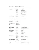
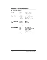
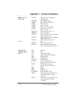
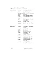
EIDEb (ATA-2),

IOCS16b_

Indicates a 16-bit register has

TLL levels

been decoded

DMARQb

Drive DMA request

DMAKb_

Drive DMA acknowledge

DIORb_

Drive I/O read

DIOWb_

Drive I/O write

DASPb_

Drive active/slave present

IORDYb

Indicates drive is ready 
for I/O cycle(s)

DD[15:0]b

Drive data lines, bits 15--0

DRESETb_

Drive reset signal

CS1FXb_

Chip select drive 0, also command
register block select

CS3FXb_

Chip select drive 1, also command
register block select

DA[2:0]b

Drive register and data port

address 

lines

INTRQb

Drive interrupt request

PDIAGb_

Passed diagnostics output from 
drive 1 and  monitored by drive 0

SCSI, XT310

ATN_

Attention

SPI/single ended

BSY_

Busy

levels

C/D_

Command or Data

I/O_

Input or Output data direction

MSG_

Message phase

ACK_

Acknowledge

SCD[15:0]_

SCSI data lines

SCDPH_

SCSI parity high byte,
provides parity for SCD[15:8]

SCDPL_

SCSI parity low byte,
provides parity for SCD[7:0]

SEL_

Select

REQ_

Request

SRST_

SCSI bus reset

TERMPWR

SCSI terminator power

NDET_

Narrow detect, may be pulled low 
to indicate that bits [7:0] are
connected

WDET_

wide detect, may be pulled low to 
indicate that bits [15:8] are

connected

Summary of Contents for G8

Page 1: ...G8 CPCI Enclosure User s Guide G8 8 Slot CompactPCI Enclosure User s Guide 095 30004 00 Rev A ...

Page 2: ...ny mechanical electronic or other means in any form without prior written permission of the manufacturer Trademarks IBM PC is a registered trademark of International Business Machines Corporation Intel and Pentium are registered trademarks of Intel Corporation Award is a registered trademark of Award Software Inc Other product names mentioned herein are used for identification purposes only and ma...

Page 3: ...G8 CPCI Enclosure User s Guide 3 Thank You from the team for purchasing this product I Bus Phoenix Power and Computing Systems ...

Page 4: ...com Please be sure to include your name the name of your company the product purchased and the manual number revision ie 00 00000 00 Rev This number is located on the title page At I Bus Phoenix we value our customers and partners and you can continue to count on I Bus Phoenix to be customer focused and to provide you a large range of solutions from cost effec tive to fully customized industrial c...

Page 5: ...s 2 3 Backplane 2 4 Fan Plenum and Chassis Fan 2 5 Chassis Filters 2 7 Chapter 3 Power Distribution Power Supplies 3 1 Input Circuit Breaker 3 2 Chapter 4 Drive Bay Removing Installing the Drive Module 4 1 Removing Installing the Hard Drive in the Drive Module 4 2 Removing Installing the Floppy Drive in the Drive Module 4 3 Chapter 5 Specifications Specifications 5 1 Environmental Specifications 5...

Page 6: ...in Assignments A1 7 P4 Signal Descriptions A1 7 P5 Connector Pin Assignments A1 10 P5 Signal Descriptions A1 10 P4 Connector Pin Assignments Computer Telephony Bus A1 13 P4 Signal Descriptions Computer Telephony Bus A1 13 Appendix 2 Glossary of Terms Appendix 3 Limited Warranty Appendix 4 FCC Compliance List of Figures Figure 1 1 G8 Enclosure 1 3 Figure 2 1 G8 Enclosure Rear 2 3 Figure 2 2 Fan Acc...

Page 7: ...1 P1 Connector Pin Assignments A1 1 Table A1 2 P2 Connector Pin Assignments A1 3 Table A1 3 P3 Connector Pin Assignments A1 5 Table A1 4 P4 Connector Pin Assignments A1 7 Table A1 5 P5 Connector Pin Assignments A1 10 Table A1 6 P4 Connector Pin Assignments Computer Telephony Bus A1 13 Table of Contents ...

Page 8: ...iv Table of Contents This page was intentionally left blank G8 CPCI Enclosure User s Guide ...

Page 9: ... available options your system may not contain all of the features described in this manual This chapter is divided into three sections About this manual Explains how this manual is laid out and what to expect to find in it Preparing the system Defines the items included with your system and describes the procedure for unpacking and setting up the G8 Features Provides a brief overview of the major...

Page 10: ...es a glossary of the terms used in this manual Appendix 3 Limited Warranty Appendix 4 FCC Information Preparing the System CAUTION Unpacking the system Unpack your system at a static free workstation while observing proper Electrostatic Discharge ESD practices I Bus Phoenix reserves the right to refuse warranty service on units improperly unpacked to protect against ESD damage Included with your G...

Page 11: ... The G8 is equipped with an 8 slot CompactPCI passive backplane Power supply The G8 can be equipped with up to two current sharing redundant 350W AC or DC power supplies Drive module The G8 mounts one 3 5 inch hard drive one 3 5 inch floppy drive and one CD ROM drive The drives module plugs directly into the backplane Optional top drive bay modules 4 5 1 4 half height drives mounted horizontally 8...

Page 12: ...1 4 Chapter 1 Introduction G8 CPCI Enclosure User s Guide This page was intentionally left blank ...

Page 13: ...fe workstation 3 Loosen the two screws on the CPU board module s front panel 4 Completely retract the injector ejector handles Note Some force may be required 5 Slide the CPU board module out of the chassis 6 Using the module guides slide the new CPU board into the chassis making sure to align the two guide pins with their card guides inside the chassis 7 Engage the injector ejector handles by pre...

Page 14: ...orkstation 3 Retract the injector ejector handles of the add in board module 4 Slide the add in board module out of the chassis 5 Using the module guides slide the new add in board into the chassis making sure to align the two guide pins with their card guides inside the chassis 6 Engage the injector ejector handles by pressing them towards each other Note If you do not plan on immediately replaci...

Page 15: ...panel as much as possible Note The screws are captive to the front panel and cannot be completely removed 4 Completely retract the injector ejector handles Note This may require some force 5 Slide the rear I O module out of the chassis 6 Using the module guides slide the new rear I O module into the chas sis making sure to align the two guide pins with their card guides inside the chassis 7 Engage...

Page 16: ...ns 7 Turn on the main system power Backplane The G8 supports an 8 slot CPCI backplane accessible by removing the top of the chassis See the back of this manual or the backplane manual for charts providing connector information for the CompactPCI backplane 1 Turn off the main system power 2 Place the chassis on an ESD safe workstation 3 Remove the CPU board power supply module s drive module all ad...

Page 17: ...hassis using the thirty six screws removed in step 3 8 Secure the rear plate to the chassis 9 Install the CPU board power supply module drive module all add in boards and all rear I O modules if applicable 10 Turn on the main system power Fan Plenum and Chassis Fan 2 5 G8 CPCI Enclosure User s Guide Figure 2 2 Fan Access Door and Fan Tray Captive Thumb Screw Fan Tray ...

Page 18: ...se the access door and tighten the two captive thumb screws Removing installing a fan 1 Remove the fan tray 2 Remove the four screws securing the fan and its two finger guards to the fan tray taking care not to lose any of the eight flat washers 3 Swap out the old fan for a new one and place it between the two fin ger guards Note The arrow indicating the fan air direction 4 Secure the new fan and ...

Page 19: ...the two captive thumb screws located on both sides of the fan access door at the front of the chassis 2 Open the access door 3 Remove the filter from the filter plate and clean it 4 Replace the filter in the filter plate completely close the fan access door Note This may require some force 5 Tighten the captive thumb screws Figure 2 3 Fan Sub Assembly Air Direction 2 7 G8 CPCI Enclosure User s Gui...

Page 20: ...2 8 G8 CPCI Enclosure User s Guide Chapter 2 Hardware This page was intentionally left blank ...

Page 21: ...e system provided the remaining supply is sufficient to power all of the CPU and add in cards installed in the system Removing and installing the power supply module 1 Loosen the two screws on the power supply module s front panel as much as possible Note The screws are captive to the front panel and cannot be complete ly removed 2 Completely retract the injector ejector handles Note This may requ...

Page 22: ...ews that mount the breaker plate to the rear panel 4 Gently pull the breaker plate away from the rear panel until the circuit breaker and the quick disconnect terminals can be easily accessed 5 With the wires still connected squeeze the spring clips on the sides of the old circuit breaker pushing it through the front of the breaker plate until it pops out the front of the plate 6 Removing the wire...

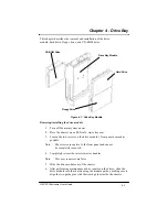
Page 23: ...le s front panel as much as possible Note The screws are captive to the front panel and cannot be completely removed 4 Completely retract the injector ejector handles Note This may require some force 5 Slide the drive module out of the chassis 6 After performing maintenance and or repairs on the drives slide the drive module into the chassis using the module guides making sure to align the two gui...

Page 24: ...t tak ing care not to lose any of the eight nylon shoulder washers Note These washers isolate the hard drive case from chassis ground If they are not replaced in their proper positions EMI RFI integri ty may be compromised 6 Remove the hard drive 7 Place a new hard drive on the bracket after first placing four shoulder washers in the drive mounting holes with the flat washer side toward the hard d...

Page 25: ...ssis ground If they are not replaced in their proper positions EMI RFI integri ty may be compromised 6 Remove the floppy drive 7 Place a new floppy drive on the bracket after first placing four shoul der washers in the drive mounting holes with the flat washer side toward the floppy drive 8 Place the other four shoulder washers in the drive mounting holes with the flat washer side toward the mount...

Page 26: ...4 4 This page was intentionally left blank Chapter 4 Drive Bays G8 CPCI Enclosure User s Guide ...

Page 27: ...ot wide 1 Drive Module 3 slots wide 2 Power Supply Locations 2 slots wide each Cooling 3 fans 85 CFM each Dimensions Height 17 14 no top drive module 22 32 4 drive module 23 92 8 drive module Width 17 10 Depth 11 69 Input voltage 105 126 VAC or 210 252 VAC auto ranging Optional 48VDC input Output voltage 40A 5VDC 25A 3 3VDC 9A 12VDC 2A 12VDC 350W total per power supply ...

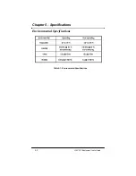
Page 28: ...5 2 Chapter 5 Specifications G8 CPCI Enclosure User s Guide Environmental Specifications Table 5 1 Environmental Specifications ...

Page 29: ...wer V I O 5V or 3 3V power GND to digital signal ground plane PCI_RST_ Master reset PCI Bus Signals AD 31 0 32 bit Address Data bus C BE 3 0 _ Command Byte Enable bus PAR Bus parity BRSVPxxx PCI bus reserved signals PCIbus arbitration GNT0_ Bus grant 0 signals REQ0_ Bus request 0 Interrupt Request INTA_ INTB_ INTC_ INTD_ Signals Table A1 1 P1 Connector Pin Assignments system slot ...

Page 30: ...eporting signals SERR_ System Error PCI bus speed signals M66EN 66MHz bus enable PCI bus clock CLK0 System Management IPMB_SCL Bus IPMB_SDA IPMB_PWR 64 bit Extension REQ64_ Request 64 bit Transfer Signals ACK 64_ Acknowledge 64 bit Transfer JTAG Boundary TCK Test Clock Scan Signals TDI Test Input TDO Test Output TMS Test Mode Select TRST_ Test Reset IDE Interrupts INTP Primary Interrupt IRQ14 INTS...

Page 31: ...G8 CPCI Enclosure User s Guide A1 3 Appendix 1 Technical Reference P2 Connector Pin Assignments Table A1 2 P2 Connector Pin Assignments system slot ...

Page 32: ...extension C BE 4 7 _ Command Byte Enable bus PAR64 64 bit Bus parity BRSVPxxx PCI bus reserved signals PCI bus arbitration GNT 6 1 _ Bus grants signals REQ 6 1 _ Bus requests PCI bus clocks CLK 6 1 Miscellaneous signals PRST_ Push Button Reset DEG_ Degrade signal Power Supply FAL_ Supply Fail Signal Power Supply GA 4 0 Geographic Addressing SYSEN_ System slot identification 64EN_ 64 bit bus enable...

Page 33: ...CBE 3 0 _ Command Byte Enable bus PPAR Bus parity Primary PCI bus PGNT 6 0 _ Bus grants arbitrations signals PREQ 6 0 _ Bus requests Primary PCI bus PFRAME_ Cycle Frame transaction control PTRDY_ Target Ready signals PIRDY_ Initiator Ready PSTOP_ Target Initiator transaction stop bit PLOCK_ Resource Lock bit PDEVSEL_ Devise Select A1 5 G8 CPCI Enclosure User s Guide Table A1 3 P3 Connector Pin Ass...

Page 34: ...1 Technical Reference Primary PCI bus PPERR_ Data Parity Error error reporting PSERR_ System Errors signals Primary PCI bus PCLK 6 0 clocks I2C signals PSDAT PSCK PSALRT Miscellaneous Signals WDRST_ Watch Dog circuit reset FAN1 2 Fan tach outputs ...

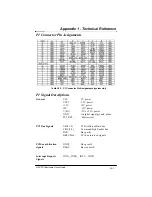
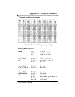
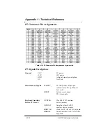
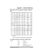
Page 35: ...b_ DA1b GND DA0b DA2b GND 22 GND GND IORDYb NU DMAKb_ INTRQb GND 21 GND DMARQb GND DIOWb_ GND DIORb_ GND 20 GND DD14b DD0b DD15b GND PDIAGb _ GND 19 GND DD3b DD12b DD2b DD13b DD1b GND 18 GND DD9b_ DD5b DD10b DD4b DD11b GND 17 GND DRESETb_ GND DD7b DD8b DD6b GND 16 GND ETX1 ETX1 SRX1 SRX1 GND GND 15 GND GND VCC VCC NU NU GND Key 12 14 11 GND BLUE DACVSS NU GND GND GND 10 GND TERMPWR HSYNC VSYNC RED...

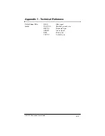
Page 36: ...ister block select DA 2 0 b Drive register and data port address lines INTRQb Drive interrupt request PDIAGb_ Passed diagnostics output from drive 1 and monitored by drive 0 SCSI XT310 ATN_ Attention SPI single ended BSY_ Busy levels C D_ Command or Data I O_ Input or Output data direction MSG_ Message phase ACK_ Acknowledge SCD 15 0 _ SCSI data lines SCDPH_ SCSI parity high byte provides parity f...

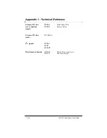
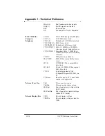
Page 37: ...endix 1 Technical Reference VGA Video VGA BLUE Blue signal levels DACVSS Shielded ground wire HSYNC Horizontal sync GREEN Green signal RED Red signal VSYNC Vertical sync A1 9 G8 CPCI Enclosure User s Guide ...

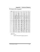
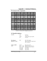
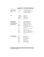
Page 38: ...laneous Signals SPKROC_ PC AT speaker output open collector may have pull up on host card RESET_ System reset output TTL totem pole Keyboard Auxilary AUXCLK Clock for PS 2 auxiliary Device TTL levels device mouse AUXDAT Serial data line for PS 2 auxilary device mouse KBDCLK Clock for PC AT or PS 2 keyboard KBDDAT Serial data line for PC AT or PS 2 keyboard Table A1 5 P5 Connector Pin Assignments s...

Page 39: ...nter defined when used in cannot accept more data EPP ECP modes ERR_ Peripheral detected an error PD 7 0 Parallel data lines bits 7 0 PE Paper end indicates the printer is out of paper AFD_ Auto feed causes printer to line feed INIT_ Initializes the printer SLIN_ Select in selects the printer STB_ Data strobe indicates data is valid SLCT Select peripheral indicates it is selected Serial COM Ports ...

Page 40: ...A_ Write data to drive WGATE_ Enables head write circuitry of drive WPROT_ Indicates a disk is write protected EIDEa ATA 2 IOCS16_ Indicates a 16 bit register has been decoded DMARQ Drive DMA request DMAK_ Drive DMA acknowledge DIOR_ Drive I O read DIOW_ Drive I O write DASP_ Drive active slave present IORDY Indicates drive is ready for I O cycle s DD 15 0 Drive data lines bits 15 0 DRESET_ Reset ...

Page 41: ...gnal Descriptions Computer Telephony Bus General VCC 5V power VCC3 3 3V power V I O 5V or 3 3V power 12V 12V power 12V 12V power GND To digital signal ground plane FG To chassis frame ground A1 13 G8 CPCI Enclosure User s Guide Table A1 6 P4Connector Pin Assignments Computer Telephony Bus ...

Page 42: ..._NETREF_2 Secondary 8kHz 1 544MHz or 2 048mhz telecom network timing reference CT_MC 2Mbps message channel FR_COMP 8kHz SCbus compatibility frame clock SCLK 8 192MHz SCbus compatibility data clock SCLKx2 Skewed 8 19MHz SCbus compati bility data clock CT_EN Logical equivalent of the CompactPCI signal BD_SEL_ on P1 CT_Reset Reset for use by CT Front Cards that do not Populate P1 Telecom Power Bus Vb...

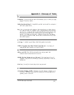
Page 43: ...s Addresses are sent over the address bus to signal a memory location and the data is transferred over the data bus to that location C card cage A cabinet or metal frame that holds printed circuit cards CMOS Complementary Metal Oxide Semiconductor A technique of arranging transistors which uses very low power D disk access LED The LED located on the front control panel that indicates when the hard...

Page 44: ...F floppy drive A device for reading the information contained on external portable computer disks called floppy disks front control panel The small panel on the front of the computer that con tains the power switch reset switch Power ON LED the disk access LED and the keyboard connector H hard drive Data storage devices Hard drives magnetically store computer data on spinning internal disks hold d...

Page 45: ...r computer power good Signal used to prevent the computer from starting until the power has stabilized The power good line switches from 0 to 5 volts within one tenth to one half second after the power supply reaches normal voltage levels Whenever low input voltage causes the output voltage to fall below operating levels the power good signal goes back to zero power ON diagnostic LED The LED locat...

Page 46: ...c interrupt used to derive local time reset switch Button or key that reboots the computer All current activities are stopped cold and any data in memory is lost retaining bracket The bracket on the back of the chassis that holds connectors from the board usually a DB9 for serial port a DB25 for paral lel port and mini DIN connectors for keyboard and mouse S SCSI Small Computer System Interface A ...

Page 47: ...ce the defective parts at purchaser s cost and deliver the defective parts to the purchaser This Limited Warranty shall not apply if the product has been misused carelessly handled defaced modified or altered or if unauthorized repairs have been attempted by others The above warranty is the only warranty authorized by I Bus Phoenix and is in lieu of any implied war ranties including implied warran...

Page 48: ...n a commercial environment This equipment generates uses and can radiate radio frequency energy and if not installed and used in accordance with the instruction manual may cause interference to radio communications Operation of this equipment in a residential area is likely to cause harmful interference in which case the user will be required to correct the interference at their own expense Change...

Reviews: