TM 11-6625-3071-14
3478A
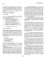
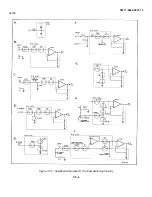
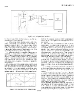
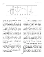
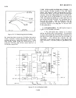
Figure 7-F-10. Runup Slopes for Zero Inputs (41/2
Digit Model)
slopes. For a perfect zero reading, the number of S + 4
slopes will be the same as the number of S-4 slopes.
This is represented in Figure 7-F-10.
7-F-38. Slope S + 4 and S-4 Generation. The following
explains how the curents for slopes S+4 and S-4 are
generated.
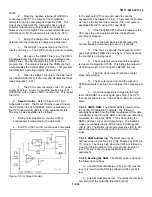
a.
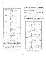
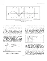
Slope S + 4. Refer to Figure 7-F-I I. Note that
both Y1 and Y2 paths are connected to ground. Since
the summing node of the paths is a virtual ground and
Y1 and Y2 are also connected to ground, no current
flows between the paths and the summing node.
Current does flow from + Vref (Positive Reference
Voltage) through a 100K ohm resistor into the integrator
capacitor (con- nected to the negative terminal of U401).
This generates a negative going output slope.
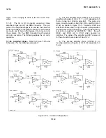
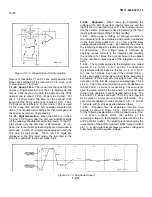
b. Slope S-4. Refer to Figure 7-F-12. Note that
both Y1 and Y2 paths are connected to -Vref (Negative
Reference Voltage). Since the summing node is a virtual
ground, current flows from + Vref through a 100K ohm
Figure 7-F-11. Slope S+4 Generation
resistor and paths Y1 and Y2 to -Vref. Current also flows
from the integrator capacitor (C) to -Vref. This current is
generated because the total resistance of the Y1 and Y2
paths is smaller than the 100K ohm resistor from + Vref.
The current from + Vref plus the current from the
capacitor equals the total current through paths Y1 and
Y2. Since the total resistance of paths Y1 and Y2 is 50K
ohms, the current from + Vref (II) and the current from
the capacitor (I2) is half as large as the total YI and Y2
current (13). The resultant output slope is positive.
Figure 7-F-12. Slop S-4 Generation
7-F-39. Slope S + 0 and S-O Generation. Refer to
Figure 7-F-13. Note that one side of a IOOK ohm
resistor (YI path) is connected to ground and the other
side is con- nected to the summing node. Since the
100K ohm resistor from +Vref (Y3 path) and the IOOK
ohm resistor from -Vref (Y2 path) are also connected to
the summing node, no current flows from the integrator
capacitor (C). This is because the resistance value of
path Y2 and Y3 is the same and makes the current value
of paths Y2 and Y3 the same (but opposite polarity).
This is true for both slopes S + 0 and S-0. The only dif-
7-F-12
Summary of Contents for 3478A
Page 2: ...TM 11 6625 3071 14 A ...
Page 4: ...TM 11 6625 3071 14 C D BLANK ...
Page 12: ...TM 11 6625 3071 14 Table 1 1 Specification 1 2 ...
Page 13: ...TM 11 6625 3071 14 Table 1 1 Specifications Cont 1 3 ...
Page 14: ...TM 11 6625 3071 14 Table 1 1 Specifications Cont 1 4 ...
Page 53: ...TM 11 6625 3071 14 1 ...
Page 54: ...TM 11 6625 3071 14 2 ...
Page 55: ...TM 11 6625 3071 14 3 ...
Page 56: ...TM 11 6625 3071 14 4 ...
Page 87: ...TM 11 6625 3071 14 3478A Figure 7 D 3 Flowchart B 7 D 5 ...
Page 88: ...TM 11 6625 3071 14 3478A Figure 7 D 4 Flowchart C 7 D 6 ...
Page 91: ...TM 11 6625 3071 14 3478A Figure 7 D 6 Flowchart D 7 D 9 ...
Page 111: ...TM 11 6625 3071 14 Figure 7 F 17 3478A Simplified Reference Circuitry 7 F 16 ...
Page 122: ...TM 11 6625 3071 14 Table A 2 A 2 HP IB Worksheet A 4 ...
Page 137: ...TM 11 6625 3071 14 Figure 7 D 2 Flow chart A 7 D 3 ...
Page 139: ...TM 11 6625 3071 14 Figure 7 G 2 3478A Block Diagram 7 G 3 ...
Page 140: ...TM 11 6625 3071 14 Component Locator for Input Circuitry and Ohms Current Source 7 G 4 ...
Page 141: ...TM 11 6625 3071 14 Figure 7 G 3 Input Circuitry and Ohms Current Source 7 G 5 ...
Page 142: ...TM 11 6625 3071 14 F G 6 ...
Page 143: ...TM 11 6625 3071 14 2 Figure 7 G 4 AC to DC Converter 7 G 7 ...
Page 144: ...TM 11 6625 3071 14 Component Locator for A D Converter and Control Logic 7 G 8 ...
Page 145: ...TM 11 6625 3071 14 3 Figure 7 G 5 A D Converter and Control Logic 7 G 9 ...
Page 146: ...TM 11 6625 3071 14 7 G 10 ...
Page 147: ...TM 11 6625 3071 14 4 Figure 7 G 6 Power Supplies 7 G 11 7 G 12 blank ...
Page 148: ......
Page 149: ...PIN NO 057444 ...


