background image

E2 - 8

3.3

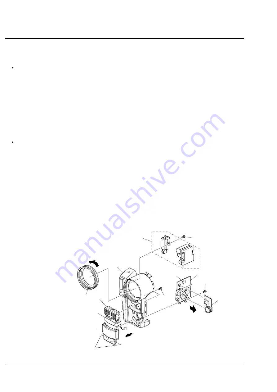
Jack Cover, Flash Unit, JKR Circuit Board, JKF Circuit Board, Microphone, IR Filter, Lens

Hood, Front Case (Fig. 3-3)

Caution when disassembling:

Caution when disassembling:

Caution when disassembling:

Caution when disassembling:

Caution when disassembling:

The flash circuit board and flash emitter block have been assembled as a flash unit: Disassemble or reassemble them
together. Be careful not to damage the cable between the flash circuit board and flash emitter block.

3.3.1

3.3.1

3.3.1

3.3.1

3.3.1 Jack cover (A), Flash unit (B)

Jack cover (A), Flash unit (B)

Jack cover (A), Flash unit (B)

Jack cover (A), Flash unit (B)

Jack cover (A), Flash unit (B)

(1) While releasing the two tabs, remove the jack cover (A) in the direction of the arrow.
(2) Remove the screw holding the flash unit (B) (flash emitter block).

3.3.2

3.3.2

3.3.2

3.3.2

3.3.2 JKR circuit board (C), JKF circuit board (D)

JKR circuit board (C), JKF circuit board (D)

JKR circuit board (C), JKF circuit board (D)

JKR circuit board (C), JKF circuit board (D)

JKR circuit board (C), JKF circuit board (D)

(3) Disconnect one connector on the JKR circuit board (C).
(4) Remove the two screws holding the JKR circuit board (C) and JKF circuit board (D).
(5) While disconnecting the connection with the JKR circuit board (C), remove the JKF circuit board (D) in the direction of the

arrow.

Caution when reinstalling:

Caution when reinstalling:

Caution when reinstalling:

Caution when reinstalling:

Caution when reinstalling:

Connect the JKR circuit board (C) to the JKF circuit board (D) securely.

3.3.3

3.3.3

3.3.3

3.3.3

3.3.3 Microphone (E), IR filter (F), Lens Hood (G), Front case (H)

Microphone (E), IR filter (F), Lens Hood (G), Front case (H)

Microphone (E), IR filter (F), Lens Hood (G), Front case (H)

Microphone (E), IR filter (F), Lens Hood (G), Front case (H)

Microphone (E), IR filter (F), Lens Hood (G), Front case (H)

(6) Remove the two screws holding the microphone (E), and then remove the microphone (E) and IR filter (F) from the front

case (G).

(7) Remove the IR filter (F) from the microphone (E) in the direction of the arrow.
(8) Turn the lens hood (G) in the direction of the arrow and remove the lens hood (G) from the front case (H).

Fig. 3-3

Fig. 3-3

Fig. 3-3

Fig. 3-3

Fig. 3-3

B

H

E

F

A

(2)

(1)

(7)

(6)

(3)

C

D

(4)

G

(1)

(5)

(8)

A

A

A

A

:

Jack Cover

B

B

B

B

:

Flash Unit

C

C

C

C

:

JKR Circuit Board

D

D

D

D

:

JKF Circuit Board

E

E

E

E

:

Microphone

F

F

F

F

:

IR Filter

G

G

G

G

:

Lens Hood

H

H

H

H

:

Front Case

Summary of Contents for DZMV100E

Page 1: ...E MANUAL SERVICE MANUAL SERVICE MANUAL SERVICE MANUAL SPECIFICATIONS AND PARTS ARE SUBJECT TO CHANGE FOR IMPROVEMENT Digital Media Products Division DVD VIDEO CAMERA RECORDER 2001 March SM7108 DZMV100E DZMV100EAU DZMV100EUK ...

Page 2: ...ng This manual does not include the schematic diagrams of SHD RAM2LD and PHD circuit boards since these boards are included in the mechanism unit and they or their components are not assigned as service parts Many electrical and mechanical parts have special safety related characteristics These are often not evident from visual inspection nor can the protection afforded by them necessarily be obta...

Page 3: ...ematic diagrams 2 Values in schematic diagrams Item Value Tolerance Power capacitance Indication No indication K k M M No indication 5 All tolerances other than 5 are indicated in schematic diagrams No indication 1 8W 1 16W for leadless resistors without indication All capacitances other than the above are indicated in schematic diagrams Capacitors Capacitors Capacitors Capacitors Capacitors Item ...

Page 4: ... Switch Unit E2 10 3 7 Link Bracket R Link Bracket L Loader Mechanism Unit E2 12 3 8 Lock Unit Side Case R E2 14 3 9 GYR Circuit Board SEN Circuit Board Sensor Lens E2 14 CONTENTS CONTENTS CONTENTS CONTENTS CONTENTS 3 10 Eye Control EVF F Case Plate F EVF B Case EVF LCD EVF Backlight EBL Circuit Board E2 16 3 11 B W LCD LCD Power Unit LCD Frame Backlight Color LCD LCD B Case E2 17 4 Disassembly Wh...

Page 5: ...RAMS SCHEMATIC DIAGRAMS INTERNAL WIRING DIAGRAM 6 1 SENSOR SEN 6 3 GYRO GYR 6 4 EVF BACK LIGHT EBL 6 5 JACK F JKF 6 6 JACK R JKR 6 7 CIRCUIT BOARD DIAGRAMS SEN 6 9 GYR 6 9 EBL 6 10 ANA SIDE A 1 6 11 ANA SIDE B 1 6 13 DIG SIDE A 1 6 15 DIG SIDE B 1 6 17 JKF 6 19 JKR 6 19 SHD 2 6 20 RAM2LD 2 6 20 PHD 2 6 21 BLOCK DIAGRAMS AV PROCESS SECTION 6 23 8cm DVD RAM DRIVE SECTION 6 25 1 The circuit board dia...

Page 6: ...g standard MPEG audio Still Simultaneous recording conforming to DVD video recording standard and JPEG 1 280 960 pixels Audio playback format MPEG Dolby AC3 Recording medium 8 cm DVD RAM disc conforming to DVD RAM Book 2 1 Jacks Video Audio output 1 S video output 1 External microphone input 1 Digital input output terminal connected to PC USB jack 1 Battery system Lithium ion Power consumption app...

Page 7: ...of media Diameter of media Diameter of media Capacity per side Capacity per side Capacity per side Capacity per side Capacity per side Laser wavelength NA Laser wavelength NA Laser wavelength NA Laser wavelength NA Laser wavelength NA Recording format Recording format Recording format Recording format Recording format Track format Track format Track format Track format Track format Track pitch Tra...

Page 8: ...ed by Hitachi Capacity Capacity Capacity Capacity Capacity per side both sides per side both sides per side both sides per side both sides per side both sides Laser wavelength NA Laser wavelength NA Laser wavelength NA Laser wavelength NA Laser wavelength NA Write rate Write rate Write rate Write rate Write rate Rewritable use Rewritable use Rewritable use Rewritable use Rewritable use Cartridge C...

Page 9: ... the disc provided Removing the disc Removing the disc Removing the disc Removing the disc Removing the disc 1 1 1 1 1 Release the lock pins of cartridge Release the lock pins of cartridge Release the lock pins of cartridge Release the lock pins of cartridge Release the lock pins of cartridge The two lock pins are at the bottom left corners of sides A and B Use a fine tipped pen to slide the lock ...

Page 10: ... the following Before replacing the disc in cartridge make sure that disc surfaces are not scratched and that no dirt or fingerprint adheres to them Do not record edit or delete on the disc when scratches dirt or fingerprints cannot be removed even if disc surface is cleaned When replacing the disc in cartridge insert it until a click is heard Writing similar to recording is be performed even with...

Page 11: ... operation Will delete all still files on disc Copy necessary still files to PC etc Purpose To delete still JPEG files to be played back on PC from the disc without using PC When recording stills this DVD video camera recorder stores both stills to be played back on the video camera recorder and stills to be played back on PC Only the still files to be played back on the video camera recorder can ...

Page 12: ...ow in Fig 3 4 constitute the error codes If the ENTER button is pressed from the screen in Fig 3 4 the screen in Fig 3 5 will appear this has nothing to do with this function Notes Notes Notes Notes Notes 1 Operation display is possible without disc inserted 2 Simultaneously press the Display and STOP buttons to exit the error code display and restore normal status 3 Each time the ENTER button is ...

Page 13: ...pace Note Note Note Note Note The above defect may occur if power is shut off while data is being written to the file Operation procedure 1 Insert the disc whose RX file is to be deleted and press the DISC NAVIGATION button making sure that the DVD video camera recorder enters the disc navigation mode 2 Simultaneously press the following three buttons SHIFT DISC NAVIGATION reverse skip search 3 A ...

Page 14: ...ed control files 1 The message appears when reading recorded files or writing data to files is not possible If the message still appears after the disc is replaced with normal one there is a problem in the DVD video camera recorder This appears when user is operating information control files The message appears when reading recorded files or writing data to files is not possible If the message st...

Page 15: ... without editing on this DVD video camera recorder 1 scene will make up 1 EP or 1 CELL If scenes are combined the number of EPs will decrease but the number of CELLs will not decrease If CELL is to be divided at the upper limit number of CELLs several scenes must be deleted in this status without traversing multiple CELLs 2 Same as above This appears if a disc in which EP is not attached to the be...

Page 16: ...ixed in The repaired data may be different from the original recorded content because of partial deletion of defective portion Since the date time for repair is added to the repaired data only the corrected portion for partial repair the original date time information will be lost Since all movies and then all stills are repaired the order of recorded contents will be lost In case of message 3 onl...

Page 17: ...er is shut off during movie recording This function will repair some files when the DVD video camera recorder is restarted Since it may take 10 20 minutes for file repair work the DVD video camera recorder must be stably powered using AC adapter The message will appear at this time Note that if power is again shut off while files are being repaired restoration of those files being repaired will no...

Page 18: ...y for reference Estimate the Troubleshooting due to check results method from the symptom and try replacing circuit boards components etc as needed If it is absolutely necessary to confirm check points etc pull them out from circuit boards using lead wires etc 2 This troubleshooting guide describes only major defects The listed causes of defects and troubleshooting may not always apply 3 Troublesh...

Page 19: ...KR B TL6092 JKR B Microphone jack JK6051 JKR B PG1503 4 ANA A PG1503 5 ANA A TL1503 ANA A TL1501 ANA A Troubleshooting due to check results Troubleshooting due to check results Troubleshooting due to check results Troubleshooting due to check results Troubleshooting due to check results NG F0501 fuse faulty Replace ANA circuit board NG F0502 fuse faulty Replace ANA circuit board NG F0503 fuse faul...

Page 20: ...m or IC2001 CODEC system faulty Replace DIG circuit board No Check connections between DIG circuit board and mechanism unit IC4001 or clock circuit for IC4001 faulty Replace DIG circuit board IC4001 ATAPI system or IC2001 CODEC system faulty Replace DIG circuit board Replace mechanism unit Check connections between DIG circuit board and mechanism unit If no abnor mality is found replace mechanism ...

Page 21: ...camera block optical system time battery input output selection etc 6 2 How to update The firmware can be updated by simply setting the DVD RAM disc developed exclusively for updating in the video camera recorder the DVD RAM disc will be supplied by the factory 1 Connect the AC adapter to the video camera recorder insert the firmware updating disc into the video camera recorder and turn power on 2...

Page 22: ...ermediate Frequency or Interface INDI Indicator INST Instant INT Internal INV Inverter I O In Out Input Output A A A A A A A Analog ACC Automatic Color Control A D Analog to Digital Converter ADD Adder ADP Adapter AC Adapter ADRS Address A DUB Audio Dubbing AF Automatic focus Autofocus AFC Automatic Frequency Control AGC Automatic Gain Control AGC KILLER AGC Killer Voltage AI Automatic Intelligenc...

Page 23: ...D Liquid Crystal Display LIN Linear LNC Line Noise Canceller LOG Logarithm LP Long Play LPF Low pass Filter L R Left Right LUMA Luminance M M M M M MAN Manual M BRAKE Main Brake M CUT Monitor Cut MEM Memory MIC Microphone MIX Mixer MMV Monostable Multivibator MOD Modulator MPEG Noving Picture coding Experts Group M STATE Mechanism State M STOP Memory Stop N N N N N NEG Negative NFB Negative Feed B...

Page 24: ...do the following Be sure not to do the following Short circuit battery terminals Short circuit battery terminals Short circuit battery terminals Short circuit battery terminals Short circuit battery terminals Disassemble or modify the battery Disassemble or modify the battery Disassemble or modify the battery Disassemble or modify the battery Disassemble or modify the battery Throw the battery int...

Page 25: ... Instruction Manual Extract from the Instruction Manual Extract from the Instruction Manual Extract from the Instruction Manual Extract from the Instruction Manual For DZ MV100E For DZ MV100E For DZ MV100E For DZ MV100E For DZ MV100E ...

Page 26: ...E1 21 ...

Page 27: ...E1 22 ...

Page 28: ...E1 23 ...

Page 29: ...E1 24 ...

Page 30: ...E1 25 ...

Page 31: ...E1 26 ...

Page 32: ...cuit Board 2 14 Sound Insulation sheet L 15 Rear Cover 16 Power Terminal 1 ANA and DIG circuit boards must be replaced in units of board and their components are not assigned as service parts 17 Side Case R 18 Switch Unit 19 Mechanism Mecha Shield 20 Mechanism Unit 2 21 Loader 22 Disc Cover 23 Lock Unit 2 SHD RAM2LD and PHD circuit boards are included in the mechanism unit and they or their compon...

Page 33: ...3 42 45 47 46 44 48 24 Lens Hood 25 Front Case 26 Flash Unit 27 JKR Circuit Board 28 JKF Circuit Board 29 Jack Cover 30 IR Filter 31 Microphone 32 Eye Control 33 EVF F Case 34 Plate F 35 LCD Holder 36 EVF LCD 37 EVF Backlight 38 BL Plate 39 EBL Circuit Board 40 BL Cover 41 EVF B Case 42 LCD B Case 43 Color LCD 44 Back light 45 LCD Frame 46 LCD Power Unit 47 LCD Holder 48 B W LCD ...

Page 34: ... arrows till the end Remove the components on the line before removing the target component Proceed with disassembly in the reverse direction to the arrows starting from components on right Numbers in brackets show the item number in disassembly procedure Example 1 Before removing the microphone the top cover R block L block front block JKR circuit board and JKF circuit board jack unit must previo...

Page 35: ...h ends of connector in the direction of the arrow parallel with surface of circuit board to release the lock 2 Pull out the flat cable in the direction of the arrow Type b disconnection 1 Pull up both ends of connector from the circuit board in the direction of the arrow to release the lock 2 Pull out the flat cable in the direction of the arrow Type c disconnection 1 Disconnect the connector on f...

Page 36: ...rom the top 3 Remove the two screws holding the front case E from the bottom 4 Remove the two screws holding the L block C from the bottom 5 Remove the two screws holding the R block B from the bottom 6 Remove the two screws holding the rear cover F 7 Disconnect the flat cable from the connector on the L block C 8 Disconnect the flat cable from the connector on the R block B Cautions when reinstal...

Page 37: ...e does not come into direct contact with the shaft Figs 3 2 1 3 2 2 When installing the LCD U case be careful not to catch the backlight cable on anything 3 2 2 3 2 2 3 2 2 3 2 2 3 2 2 Front block C Front block C Front block C Front block C Front block C 7 Unsolder the jumper wire on the LSP shield H 8 Disconnect one connector on the ANA circuit board I 9 Remove the two screws holding the flash ci...

Page 38: ... D 13 F LENS LENS SURFACE O RING NG OK 6 F G I H 7 A A A A A LCD U Case B B B B B LCD Block C C C C C Front Block D D D D D RUB Sheet E E E E E LCD Power Unit F F F F F Cable Cover G G G G G Shaft H H H H H LSP Shield I I I I I ANA Circuit Board J J J J J Flash Circuit Biard Flash Unit K K K K K JKR Circuit Board L L L L L Jack Cover M M M M M O Ring N N N N N Side Case L ...

Page 39: ...uit board C 4 Remove the two screws holding the JKR circuit board C and JKF circuit board D 5 While disconnecting the connection with the JKR circuit board C remove the JKF circuit board D in the direction of the arrow Caution when reinstalling Caution when reinstalling Caution when reinstalling Caution when reinstalling Caution when reinstalling Connect the JKR circuit board C to the JKF circuit ...

Page 40: ... and remove the two screws holding the EVF block A 3 4 2 Rear cover B Power terminal C 3 4 2 Rear cover B Power terminal C 3 4 2 Rear cover B Power terminal C 3 4 2 Rear cover B Power terminal C 3 4 2 Rear cover B Power terminal C 3 Disconnect one flat cable on the ANA circuit board D 4 Remove LSP shield E that is fixed by double sided adhesive tape 5 Remove the two screws holding the rear cover B...

Page 41: ...SP H which will come out on their own at this time 3 5 4 LSP Shield D Side Case L E 3 5 4 LSP Shield D Side Case L E 3 5 4 LSP Shield D Side Case L E 3 5 4 LSP Shield D Side Case L E 3 5 4 LSP Shield D Side Case L E 11 Remove the five screws holding the LSP shield D and remove the LSP shield from the side case L D 3 6 Disc Cover Switch Unit Fig 3 6 Cautions when disassembling Cautions when disasse...

Page 42: ...ULL REINSTALL REMOVE For DZ MV100E A F A F A A A A A ANA Circuit Board B B B B B Camera Block C C C C C DIG Circuit Board D D D D D LSP Shield E E E E E Side Case L F F F F F Sound Insulation Sheet L G G G G G Ground Plate A H H H H H Heat Radiating Rubber CSP I I I I I Ground Plate F A A A A A Disc Cover B B B B B Switch Unit C C C C C Hand Strap D D D D D Side Case R E E E E E Plate of Side Case...

Page 43: ...when reinstalling Caution when reinstalling Check the arm and shaft installation positions on link brackets R L see Fig 3 7 2 The link brackets R L are symmetrical on the right and left and must be installed in the same way 3 7 2 Loader C Mechanism unit D 3 7 2 Loader C Mechanism unit D 3 7 2 Loader C Mechanism unit D 3 7 2 Loader C Mechanism unit D 3 7 2 Loader C Mechanism unit D 2 Remove the tap...

Page 44: ...4 6 1 1 a H H I B 5 a D I I Fig 3 7 2 Fig 3 7 2 Fig 3 7 2 Fig 3 7 2 Fig 3 7 2 A A A A A Link Bracket R B B B B B Link Bracket L C C C C C Loader D D D D D Mechanism Unit E E E E E Thermal Transfer Material F F F F F Mecha Shield G G G G G Link H H H H H Boss of Side Case R I I I I I Plate of Side Case R ...

Page 45: ...g Cautions when disassembling Do not disassemble any of the components inside the lens Do not subject the sensor lens or crystal filter to impact or allow them to be damaged Be careful that no foreign object such as dust enters the lens Be careful not to damage any of the connector cables flat cables 3 9 1 3 9 1 3 9 1 3 9 1 3 9 1 GYR circuit board A GYR circuit board A GYR circuit board A GYR circ...

Page 46: ...oard B in parallel using the screws and then solder the sensor C The crystal filter G used in this video camera recorder does not have an orientation 3 9 3 3 9 3 3 9 3 3 9 3 3 9 3 Lens D Lens D Lens D Lens D Lens D 8 Remove the screw holding the lens front frame I Cautions when reinstalling Cautions when reinstalling Cautions when reinstalling Cautions when reinstalling Cautions when reinstalling ...

Page 47: ...ection of the arrow 4 While widening plate F C remove it in the direction of the arrow 3 10 3 EVF B case D EVF LCD E EVF backlight F EBL Circuit board K 3 10 3 EVF B case D EVF LCD E EVF backlight F EBL Circuit board K 3 10 3 EVF B case D EVF LCD E EVF backlight F EBL Circuit board K 3 10 3 EVF B case D EVF LCD E EVF backlight F EBL Circuit board K 3 10 3 EVF B case D EVF LCD E EVF backlight F EBL...

Page 48: ...older G 3 11 2 LCD power unit B 3 11 2 LCD power unit B 3 11 2 LCD power unit B 3 11 2 LCD power unit B 3 11 2 LCD power unit B 4 Disconnect one connector and flat cable on the LCD power unit B 5 Remove the screw holding the LCD power unit B 3 3 3 3 3 11 3 LCD frame C Backlight D Color LCD E LCD B case F 11 3 LCD frame C Backlight D Color LCD E LCD B case F 11 3 LCD frame C Backlight D Color LCD E...

Page 49: ... eye control 4 2 Removing DVD RAM Disc Important Important Important Important Important Perform the following procedure only when the disc loading block does not open DVD RAM disc cannot be removed even if the EJECT button is pressed The disc loading block of this video camera recorder will open in the normal status without power supply being connected Before disassembling Before disassembling Be...

Page 50: ...lding the front case E from the bottom 4 Remove the two screws holding the L block C from the bottom 5 Remove the two screws holding the R block B from the bottom 6 Remove the two screws holding the rear cover F 7 Disconnect the flat cable from the connector on the L block C 8 Disconnect the flat cable from the connector on the R block B Cautions when reinstalling Cautions when reinstalling Cautio...

Page 51: ...it 4 2 3 4 2 3 4 2 3 4 2 3 4 2 3 Pressing e of lock unit H Fig 4 3 Pressing e of lock unit H Fig 4 3 Pressing e of lock unit H Fig 4 3 Pressing e of lock unit H Fig 4 3 Pressing e of lock unit H Fig 4 3 9 Use tweezers etc to press portion e of lock unit H in the R block ...

Page 52: ...he cable between the DIG circuit board and LCD block and speaker cable so that they gather the cables together 5 2 DIG Circuit Board Figs 5 2 5 3 5 4 1 Paste shield materials A and B For DZ MV100A on side A see Fig 5 2 2 Paste shield material C on side B see Fig 5 3 and then paste shield material D on C see Fig 5 4 5 5 5 5 5 Information on Installation Positions of Shields etc Information on Insta...

Page 53: ...ial A on the JKF circuit board see Fig 5 7 and paste shield material B on A see Fig 5 8 making sure that B covers both the JKF and JKR circuit boards 2 Paste heat radiating rubber C on the inside of front case see Fig 5 9 3 Solder the GND cable D between the JKR circuit board E and LSP shield F see Figs 5 9 5 10 Fig 5 5 Fig 5 5 Fig 5 5 Fig 5 5 Fig 5 5 A A A A A B B B B B C C C C C Fig 5 6 Fig 5 6 ...

Page 54: ...uit board H see Fig 5 14 4 Use two screws to secure the Mecha shield F to the mechanism unit see Fig 5 14 Fig 5 10 Fig 5 10 Fig 5 10 Fig 5 10 Fig 5 10 Fig 5 9 Fig 5 9 Fig 5 9 Fig 5 9 Fig 5 9 C C C C C D D D D D F F F F F E E E E E Z Z Z Z Z Fig 5 11 Top view Fig 5 11 Top view Fig 5 11 Top view Fig 5 11 Top view Fig 5 11 Top view B B B B B Fig 5 12 Side view Fig 5 12 Side view Fig 5 12 Side view Fi...

Page 55: ... and B on the flat cable between the R and L blocks see Fig 5 15 Fig 5 14 Fig 5 14 Fig 5 14 Fig 5 14 Fig 5 14 F F F F F Fig 5 15 Fig 5 15 Fig 5 15 Fig 5 15 Fig 5 15 B B B B B A A A A A For DZ MV100A For DZ MV100A For DZ MV100A For DZ MV100A For DZ MV100A G G G G G H H H H H ...

Page 56: ...vailable DSP R Jig DSP R Jig DSP R Jig DSP R Jig DSP R Jig No 7099448 C12 Light Balancing Filter C12 Light Balancing Filter C12 Light Balancing Filter C12 Light Balancing Filter C12 Light Balancing Filter No 7099369 Personal Computer PC Personal Computer PC Personal Computer PC Personal Computer PC Personal Computer PC Goods on the Market Personal Computer Cable Personal Computer Cable Personal Co...

Page 57: ...to the monitor and if it is not terminated with 75 ohm the output video signal level cannot be measured correctly 5 Use light box that does not flicker and whose color temperature is controlled for adjustment If an inappropriate light box is used precise adjustment will not be possible and the adjustment program will not operate normally 6 Take care with the following when pointing the video camer...

Page 58: ...t for a case where some designation is given Note Note Note Note Note The names of switches knobs modes etc of oscilloscope may vary slightly depending on the manufacturer or model Since some oscilloscopes may have switches etc other than the above that must be set see the instruction manual of the particular oscilloscope for details Fig 2 1 Fig 2 1 Fig 2 1 Fig 2 1 Fig 2 1 COLOR VIDEO MONITER YEL ...

Page 59: ...justment Digital Adjustment Digital Adjustment Digital Adjustment 1 Sampling Pulse 2 Auto Iris Control 3 Shutter 4 White Balance 5 Chroma Gain 1 Zoom Focus Tracking 2 AF Noise Level Stabilizer Adjustment Stabilizer Adjustment Stabilizer Adjustment Stabilizer Adjustment Stabilizer Adjustment 3 Spot Noise Spot Noise Spot Noise Spot Noise Spot Noise Adjustment Adjustment Adjustment Adjustment Adjustm...

Page 60: ... DOS refer to the instruction manual of PC since this varies for each PC 3 The letter to be input is to designate the drive into which the adjustment floppy disk has been inserted If using a drive other than A designate the drive 4 The number to be input after a space is to designate the serial port no of PC If the PC has two or more serial ports and the DSP R jig is connected to a port other than...

Page 61: ... Important Important Important Important Important After completing this adjustment be sure to perform all adjustment items as follows Procedure 1 Input A A A A A to PC on the main menu screen 2 The screen for verifying the initialization will appear Input Y Y Y Y Y to PC 1 3 Follow the instructions on PC display thereafter 1 Entering N N N N N on the screen for verifying initialization will resto...

Page 62: ...justment Incompleted Phenomenon The picture becomes too bright The picture becomes too dark Condition Set the zoom to wide end and point at the light box without chart inserted to fill the screen Procedure 1 Input 2 2 2 2 2 to PC on the adjustment menu screen 2 Follow the instruction on PC display thereafter 3 After the AIC auto iris control adjustment complete screen appears press any key to rest...

Page 63: ...ter the screen for adjustment is in progress appears the adjustment complete screen will appear Press any key to restore the shutter adjustment menu screen 7 When using a light box Change the subject from light box to a 100W bulb type fluorescent light Set the 100W bulb type fluorescent light approx 20 cm away from the lens surface When using white paper camera light Adjust the amount of light fro...

Page 64: ...nt instruction screen B screen B screen B screen B screen B Light amount instruction Light amount instruction Light amount instruction Light amount instruction Light amount instruction screen D screen D screen D screen D screen D 100W bulb type 100W bulb type 100W bulb type 100W bulb type 100W bulb type fluorescent light fluorescent light fluorescent light fluorescent light fluorescent light Decre...

Page 65: ...Chroma Gain Adjustment Figs 5 1 5 2 5 3 Chroma Gain Adjustment Figs 5 1 5 2 5 3 Incompleted Phenomenon Color of the picture is denser than that of the subjuct Color of the picture is lighter than that of the subject Equipment Oscilloscope or Vectorscope Test Point Video Out Jack Condition Atach a C12 filter Point the at a color bar chart Procedure 1 Input 5 5 5 5 5 to PC on the adjustment menu scr...

Page 66: ...V 20 mVp p When using a vectorscope Fig 5 2 Press the D D D D D or U U U U U key to set the red vector to approx 200 of burst vector Then while holding down the Ctrl key press the D D D D D or U U U U U key to set the red vector to approx 200 5 of burst vector For DZ MV100E When using an oscilloscope Fig 5 1 Press the D D D D D or U U U U U key to set the red level on waveform to approx 600 mVp p ...

Page 67: ...o not place any obstruction between the lens and chart during adjustment Procedure 1 Input 1 1 1 1 1 to PC on the AF menu screen 2 Follow the instructions on PC display thereafter 2 2 2 2 2 AF Noise Level Adjustment AF Noise Level Adjustment AF Noise Level Adjustment AF Noise Level Adjustment AF Noise Level Adjustment Incompleted Phenomenon It takes time until a subject is brought into focus Corre...

Page 68: ...ar on the screen which are caused by a defect in pixel of CCD image sensor Perform this adjustment after specified components have been replaced see List of Adjustment Items Perform this adjustment if spot noise occurs under abnormal usage conditions or after long term use If spot noise still occurs after this adjustment is complete the CCD image sensor may be defective Perform this adjustment aft...

Page 69: ...will be restored 2 Take great care that connections between video camera recorder and PC faulty connection of jig etc unexpected power off of video camera recorder or PC etc are correct during spot noise adjustment If trouble occurs Data Initialize and other adjustments must be performed again MANUAL ADJUSTMENT PROGRAM A DATA INITIALIZE B ADJUSTMENT C AUTO FOCUS D STABILIZER E SPOT NOISE ESC END P...

Page 70: ...ry PRESS ANY KEY ERROR OCCURRED ON FDET ADJUSTMENT Supply power again and re adjust PRESS ANY KEY Check the ANA circuit board and replace it if necessary ERROR OCCURRED ZOOM DOES NOT WORK Supply power again and re adjust PRESS ANY KEY TOO BRIGHT The subject is too bright PRESS ANY KEY Move the camera further away from the light box TOO DARK The subject is too dark PRESS ANY KEY Check the light box...

Page 71: ... Check the subject 6 2 Error Message of Autofocus ERROR MESSAGE ERROR MESSAGE ERROR MESSAGE ERROR MESSAGE ERROR MESSAGE COUNTERMEASURE COUNTERMEASURE COUNTERMEASURE COUNTERMEASURE COUNTERMEASURE THIS MODEL NEED NOT BE ADJUSTED Adjustment is to be started for models that do not need adjustment PRESS ANY KEY Model selection is incorrect Initial setting for each model is incorrect Make sure of model ...

Page 72: ...G CIRCUIT BOARD 907 101 901 104 902 902 106 901 901 901 901 902 102 904 904 114 700 105 154 107 122 1 122 1 907 147 155 1 The flash circuit board and flash emitter block have been assembled as a flash light FLASH CIRCUIT BOARD FLASH EMITTER BLOCK 901 160 109 907 A A 916 916 159 159 163 157 162 156 158 902 JKF CIRCUIT BOARD JKR CIRCUIT BOARD ...

Page 73: ...4 2 1 2 3 4 A B C D E CABINET 2 140 145 901 901 901 901 913 913 913 901 901 901 901 901 141 901 901 901 901 901 901 144 MECHANISM UNIT 146 A A 166 161 914 165 165 165 ...

Page 74: ...4 3 1 2 3 4 A B C D E LCD ELECTRONIC VIEWFINDER EVF 130 129 138 137 128 134 904 904 133 901 135 901 901 EBL CIRCUIT BOARD 139 131 136 110 115 116 111 902 902 902 910 113 118 117 ...

Page 75: ...4 4 1 2 3 4 A B C D E ACCESSORIES CAMERA 801 802 DZ ACP1 803 804 805 807 808 809 810 Battery DZ BP16 902 902 902 902 125 123 124 126 127 911 911 SEN CIRCUIT BOARD GYR CIRCUIT BOARD 148 912 912 813 ...

Page 76: ...13 QD19482 HOLDER LCD 114 QD19499 CASE LCD U 115 DB10762 DISPLAY LIQWD CRYSTAL 3 5 116 DT10411 LIGHT BACK 117 HA10462 POWER UNIT 118 DB10791 DISPLAY LIQUID CRYSTAL 119 QD19992 CASE FRONT 120 GH10371 MICROPHONE 121 QX14331 FILTER IR 122 DP10351 LIGHT FLASH 123 NA30231 FRAME LENS 124 NJ12281 FRAME R 125 KQ10891 LENS ASSY 126 NX11252 RUBBER 127 UE15022 CCD IMAGE SENSOR 128 NT11792 HOLDER LCD 129 NX19...

Page 77: ... 10 25V C6052R 0893197 CERAMIC CHIP 0 022UF 10 25V C6053L 0893208 CERAMIC CHIP 1000PF 10 50V C6053R 0893208 CERAMIC CHIP 1000PF 10 50V C6090L 0893062 CERAMIC CHIP 1UF 80 20 16V C6090R 0893062 CERAMIC CHIP 1UF 80 20 16V C6091 AA00934R CERAMIC CAPACITOR 2 2UF 10 10V R1001 0790044 CHIP RESISTOR 3 3KOHM 5 1 16W R1002 0790024 CHIP RESISTOR 100 OHM 5 1 16W R1003 0790077 CHIP RESISTOR 1MOHM 5 1 16W R1005...

Page 78: ...WA D1999 5337354 DIODE MA133 D3901 5337354 DIODE MA133 IC1401 FU10323 SENSOR GYRO IC1402 FU10324 SENSOR GYRO IC1403 CK24841R IC NJU7018M IC6001 CK22341R IC NJM2112V TE1 IC6002L CK19751R ICTC7S66FU IC6002R CK19751R ICTC7S66FU IC6091 CK16271R IC BU4066BCFV E2 Q1001 5328221 TRANSISTOR 2SC2620 QC Q1002 1323279 TRANSISTOR DTC114YE Q1401 1323279 TRANSISTOR DTC114YE Q1402 1323252 TRANSISTOR XP4501 Q3901 ...

Page 79: ...G1982 PG1991 PG1002 PG1401 PG6301 PG3701 PG3702 PG3703 PG0501 EBL ANA SEN DIG JKR JKF GYR STROBO PG3801 PG1504 PG1301 PG1001 PG6001 PG1101 PG3001 PG1501 PG1502 21P CN0001 14P 2P 2P 24P 3 5 LCD PANEL BACK LIGHT 13P 21P 10P MIC LENSE UNIT JK1991 S VIDEO OUT JK6051 EXT MIC IN JK5001 USB I F JK1981 AV OUT SPEAKER BACK UP BATTERY 2P INV MODULE CHARACTOR DISPLAY LCD REVERSE SW 30P 100P 15P 12P OPERATE S...

Page 80: ...PG1101 SENSOR SEN NOTE VOLTAGES ARE MEASURED WHEN CAMERA IS POINTED AT THE COLOR BAR CHART 3 3k MN39290FH 7 0 11 4 14 8 10 8 15 0 0 4 2 7 1 5 2 0 0 07 07 TE1 To SENSOR SEN PG1002 GYRO GYR CODE PART NAME 5H XP4501 64 DTC114YE GYRO AMP VOLTAGES ARE MEASURED WHEN CAMERA IS POINTED AT THE COLOR BAR CHART 3 3 1 3 1 2 0 3 3 1 3 1 2 3 1 0 0 1 3 0 1 3 1 3 0 1 3 0 3 3 1 3 1 3 1 3 1 3 1 3 1 3 0 ...

Page 81: ...801 To LCD PANEL To BACK LIGHT 16 15 14 13 12 11 10 9 8 7 6 5 4 3 2 1 EVF BACK LIGHT EBL CODE PART NAME BR 2SC4617 FR 2SA1774 26 DTC144EE MP MA133 16V VOLTAGE READ OR WRITE MODE 5 2 5 1 4 4 0 1 9 0 7 1 4 1 4 1 9 0 7 0 3 3 R1991 A220 R1992 A220 LN1251CAL 23 X 39k 1 2 3 4 5 6 7 8 9 10 To JACK R JKR PG1982 JACK F JKF CODE PART NAME 75H MA8075 H X C Y ...

Page 82: ...A132WA MP MA133 75H MA8075 H JACK R JKR VOLTAGE READ OR WRITE MODE INNER MIC EXT MIC 6 3 6 3 6 3 6 3 50 50 50 50 AV OUT 4 9 0 MIC FILTER ON 0 MIC FILTER OFF 4 9 MIC FILTER ON 0 MIC FILTER OFF 2 5 0 2 5 2 5 2 5 4 8 1 9 0 1 4 6 4 0 0 7 1 9 2 0 0 7 0 1 2 0 0 7 0 1 0 1 0 7 2 5 4 9 0 TE1 4 9 2 2 4 9 0 3 2 2 2 0 4 4 4 7 0 4 9 3 2 2 2 3 2 0 0 4 9 2 2 2 2 4 9 0 0 0 3 0 0 3 1 0 3 0 0 2 4 3 0 0 2 4 MIC FILT...

Page 83: ...6 10 6 9 SEN GYR EBL CIRCUIT BOARD DIAGRAMS SEN GYR EBL DZ MV100A 280 SEN SIDE A SEN SIDE B TL1006 TL1005 TL1016 TL1017 TL1004 TL1003 TL1001 GYR SIDE A GYR SIDE B EBL SIDE A EBL SIDE B ...

Page 84: ...09 TL1501 TL1510 TL1503 TL1518 TL1701 TL1702 TL6302 TL6301 5 3 1 8 5 0 8 5 0 14 3 2 24 1 6 8 3 2 33 3 1 2 3 2 21 3 2 4 5 0 15 5 0 11 3 2 47 12 49 3 0 11 5 0 1 5 3 2 7 17 5 1 14 5 0 22 3 1 26 28 12 8 12 B 7 2V BATT VOL 16 5 0 1 12 1 5 0 2 B 6 12 6 11 ANA SIDE A ANA SIDE A DZ MV100A 280 ANA SIDE A CIRCUIT BOARD DIAGRAM ...

Page 85: ...Voltage values are in reading status Example 24 4 7 Terminal no voltage value TL1523 TL0520 B BATT VOL 28 7 1 43 7 1 51 7 1 63 7 1 7 7 5 3 5 0 2 7 2 14 5 0 8 5 0 53 3 4 54 3 4 55 3 1 56 3 1 60 3 2 62 3 2 12 3 0 5 3 2 1 4 8 6 3 1 11 3 1 24 28 B 44 50 3 2 58 64 1 8 38 40 5 0 52 6 5 68 12 66 15 ...

Page 86: ...04 Note Voltage values are in reading status Example 24 4 7 Terminal no voltage value 9 3 2 1 12 2 5 13 1 7 21 3 2 31 3 2 39 1 7 43 3 2 56 3 2 65 3 2 69 3 2 78 3 2 87 3 2 99 3 2 113 3 2 117 1 7 147 3 2 163 3 2 169 1 6 177 3 2 187 3 2 195 3 2 143 1 7 91 1 7 15 3 3 23 3 3 31 3 3 41 3 3 46 3 3 ...

Page 87: ...5 4 3 1 196 3 3 188 3 3 173 3 3 92 3 3 80 3 3 75 3 3 71 3 3 66 3 3 11 3 1 24 28 B 44 50 3 2 58 64 1 8 38 40 5 0 52 6 5 68 12 66 15 160 3 3 143 3 3 131 3 3 119 3 3 111 3 3 38 3 3 17 3 3 49 3 2 55 3 2 81 3 2 1 3 2 3 3 2 9 3 2 15 3 2 29 3 2 35 3 2 41 3 2 43 3 2 1 12 1 3 0 13 3 0 75 3 2 52 3 2 49 3 2 43 3 2 1 3 2 3 3 2 9 3 2 27 3 2 52 3 2 49 3 2 43 3 2 1 3 2 3 3 2 9 3 2 27 3 2 7 8 B 37 3 2 8 12 2 3 1 ...

Page 88: ...SIDE A JKR SIDE B TL6092 TL6091 SID 6 4 7 4 4 7 6 4 7 RAM2LD 1 4 8 29 4 8 21 4 7 7 4 8 8 4 8 17 4 8 25 4 8 Note Voltage values are in reading status Example 24 4 7 Terminal no voltage value Supplement Since the DVD drive is intermittently operated set to the reading status in which laser light is emitted from the pickup 110 ...

Page 89: ... 7 8 11 7 16 4 8 16 4 8 14 3 3 13 4 7 20 4 7 39 4 7 58 4 7 74 4 7 81 4 7 96 4 7 PHD SIDE B 5 4 6 12 3 3 56 4 7 77 3 3 111 3 3 121 4 7 155 3 3 157 3 3 161 3 3 165 3 3 8 3 3 2 4 7 65 4 7 37 4 7 8 4 7 8 4 7 8 4 7 8 4 7 5 4 7 5 4 7 103 4 7 100 4 8 77 4 7 174 3 3 176 4 7 5 4 6 5 4 6 8 4 6 8 4 7 8 4 7 4 4 7 3 4 7 5 4 7 5 4 7 5 4 7 18 4 8 54 4 8 90 4 8 109 3 2 126 4 8 137 4 8 144 3 3 5 4 7 Note Voltage v...

Page 90: ...O A D CONV D A CONV SPEAKER AMP AUDIO OUTPUT STEREO SPEAKER ATAPI I F DRIVER CONTROL µP DVD DSP RD CHL 8cm DVD RAM DRIVE SECTION ATAPI ATAPI I F Y C 6 75MHz CHARACTER GEN VIDEO AMP CLK R G B COM LCD BUF USB TRANCIEVER PERSONAL COMPUTER TERMINAL VIDEO OUTPUT S Y C OUTPUT 3 5 inch LCD PANEL POWER PWM CAM1 8V CAM3 3V SENSOR LCD COLOR EVF CONT 0 44 inch LCD PANEL AC ADAPTER BATTERY IC1301 IC1202 IC120...

Page 91: ... CLOSE DETECT F T ACCELEATION SENSOR AMP FRONT MOTOR OP AMP LASER DRIVER DETECT ACTUATOR DRIVER SLIDER MOTOR DRIVER SOLENOID DRIVER ANTI VIBRATION CONT RD CHL BUF RAM ATAPI I F POWER CONT TROUBLE DET DRIVE CONTROL µP DVD DSP OPTICAL SYSTEM SEPARATE TYPE 8cmDVD RAM 1 5G ATAPI CONNECTOR CAMERA SECTION RD CHL DVD RD DVD WR IC9701 IC9703 IC9501 IC9601 X9501 58 36MHz OSC IC1901 TR X9601 10 0MHz OSC IC9...

Page 92: ...89 991 80 224 Email rplan hitachi eu com Hotline 49 180 551 25 51 12ct min Email HSE DUS Service Hitachi eu com HITACHI EUROPEAB HITACHI EUROPE SRL Box 77 Via T Gulli n 39 S 164 94 KISTA 20147 MILAN SWEDEN ITALY Tel 08 562 711 00 Tel 02 487861 Fax 08 562 711 11 Fax 02 48786381 Servizio Clienti Email csgswe hitachi eu com Tel 02 38073415 Email customerservice italy hitachi eu com HITACHI EUROPE LTD...

Reviews: