background image

compensated  to  match  the  input  impedance  of  the  ver­
tical amplifier.  This can  be easily achieved as the HM203 

has a  built-in square-wave generator with a  repetition fre­

quency  of  approx.  1  kHz  and  an 

output  voltage  of


0 .2 Vpp  ± 1 %

The  method  employed  is  as  follows.  The  probe  tip  with 
its  sprung  hook  is  connected  to  the  output  eyelet 
designated  by 

CAL. 

(calibrator)  on  the  front  panel  of the 

instrument.  The 

probe trimmer


is then adjusted  by  using 

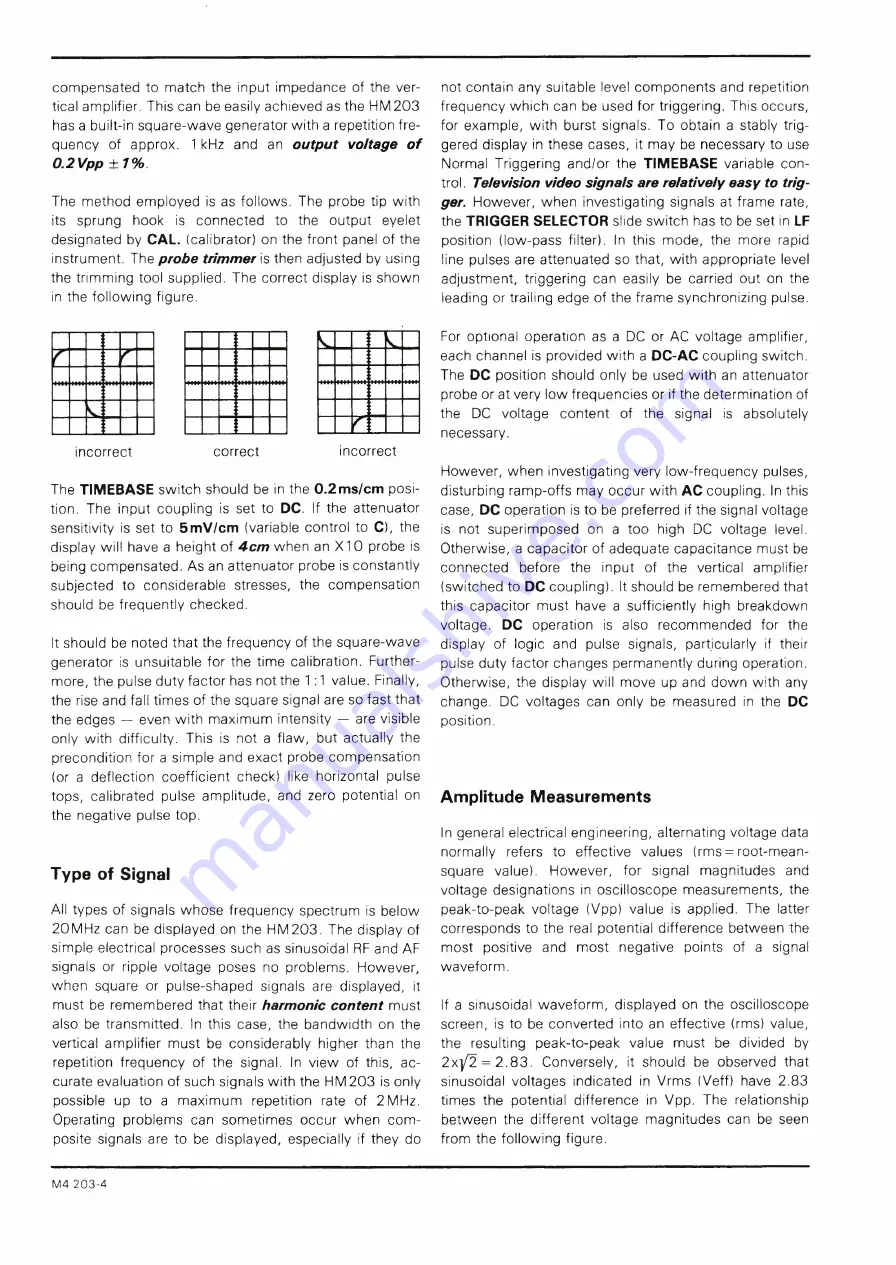
the  trimming  tool  supplied.  The  correct display  is  shown 
in  the  following  figure.

incorrect 

correct 

incorrect

The 

TIMEBASE 

switch  should  be  in  the 

0.2ms/cm 

posi­

tion.  The  input  coupling  is  set  to 

DC. 

If  the  attenuator 

sensitivity  is  set  to 

5mV/cm 

(variable  control  to 

C), 

the 

display  will  have  a  height  of 

4cm 

when  an  X I 0  probe  is 

being  compensated.  As an attenuator probe is constantly 
subjected  to  considerable  stresses,  the  compensation 
should  be  frequently  checked.

It should  be  noted  that the frequency of the square-wave 

generator  is  unsuitable  for  the  time  calibration.  Further­

more,  the pulse duty factor has not the  1:1  value.  Finally, 
the rise and fall times of the square signal are so fast that 
the  edges  —  even  with  maximum  intensity  —  are visible 
only  with  difficulty.  This  is  not  a  flaw,  but  actually  the 
precondition  for a  simple  and  exact  probe  compensation 
(or  a  deflection  coefficient  check)  like  horizontal  pulse 
tops,  calibrated  pulse  amplitude,  and  zero  potential  on 
the  negative  pulse  top.

Type  of  Signal

All  types  of  signals  whose  frequency  spectrum  is  below 

20MHz  can  be  displayed  on  the  HM203.  The  display  of 
simple electrical  processes such  as sinusoidal  RF and AF 
signals  or  ripple  voltage  poses  no  problems.  However, 
when  square  or  pulse-shaped  signals  are  displayed,  it 

must  be  remembered  that  their 

harmonic  content


must 

also  be  transmitted.  In  this  case,  the  bandwidth  on  the 
vertical  amplifier  must  be  considerably  higher  than  the 
repetition  frequency  of  the  signal.  In  view  of  this,  ac­
curate evaluation of such signals with  the  HM203  is only 

possible  up  to  a  maximum  repetition  rate  of  2 MHz. 
Operating  problems  can  sometimes  occur  when  com­
posite  signals  are  to  be  displayed,  especially  if  they  do

not contain  any  suitable  level  components and  repetition 

frequency which  can  be  used  for triggering.  This occurs, 
for  example,  with  burst  signals.  To  obtain  a  stably  trig­

gered  display  in  these  cases,  it  may  be  necessary to  use 

Normal  Triggering  and/or  the 

TIMEBASE 

variable  con­

trol. 

Television  video signals are relatively easy to  trig­

ger.


However,  when  investigating  signals  at frame  rate, 

the 

TRIGGER SELECTOR 

slide switch  has to be set in 

LF


position  (low-pass  filter).  In  this  mode,  the  more  rapid 
line  pulses  are  attenuated  so  that,  with  appropriate  level 
adjustment,  triggering  can  easily  be  carried  out  on  the 
leading  or trailing  edge  of the frame synchronizing  pulse.

For  optional  operation  as  a  DC  or  AC  voltage  amplifier, 
each  channel  is  provided  with  a 

DC-AC 

coupling  switch. 

The 

DC 

position  should  only  be  used  with  an  attenuator 

probe or at very low frequencies or if the determination of 

the  DC  voltage  content  of  the  signal  is  absolutely 

necessary.

However,  when  investigating very  low-frequency  pulses, 

disturbing  ramp-offs  may  occur with 

AC 

coupling.  In this 

case, 

DC 

operation  is to  be  preferred  if the signal voltage 

is  not  superimposed  on  a  too  high  DC  voltage  level. 
Otherwise,  a  capacitor of adequate  capacitance  must  be 
connected  before  the  input  of  the  vertical  amplifier 
(switched to 

DC 

coupling).  It should  be remembered that 

this  capacitor  must  have  a  sufficiently  high  breakdown 
voltage. 

DC 

operation  is  also  recommended  for  the 

display  of  logic  and  pulse  signals,  particularly  if  their 
pulse  duty factor changes  permanently during  operation. 
Otherwise,  the  display  will  move  up  and  down  with  any 
change.  DC  voltages  can  only  be  measured  in  the 

DC


position.

Amplitude  Measurements

In  general  electrical  engineering,  alternating  voltage  data 
normally  refers  to  effective  values  (rms = root-mean- 
square  value).  However,  for  signal  magnitudes  and 

voltage  designations  in  oscilloscope  measurements,  the 
peak-to-peak  voltage  (Vpp)  value  is  applied.  The  latter 
corresponds  to  the  real  potential  difference  between  the 

most  positive  and  most  negative  points  of  a  signal 

waveform.

If  a  sinusoidal  waveform,  displayed  on  the  oscilloscope 

screen,  is  to  be  converted  into  an  effective  (rms)  value, 
the  resulting  peak-to-peak  value  must  be  divided  by 

2x|/2 = 2.83.  Conversely,  it  should  be  observed  that 

sinusoidal  voltages  indicated  in  Vrms  (Veff)  have  2.83 
times  the  potential  difference  in  Vpp.  The  relationship 
between  the  different  voltage  magnitudes  can  be  seen 
from  the  following  figure.

r

r

\

M4  203-4

Summary of Contents for HM 203

Page 1: ...MANUAL Oscilloscope HM 2 0 3 M E S S T E C H N IK...

Page 2: ...tion adjustable on front panel Calibrator square wave generator 1kHz for probe compensation Output 0 2V 1 Regulated DC power supplies all operating voltages including the high voltage Protective syste...

Page 3: ...lifier input stages utilize monolithic integrated circuits to minimize drift Exact measurement of the displayed waveform is achieved by the 12 step frequen cy compensated input attenuator calibrated i...

Page 4: ...ith sprung hook 1C tip insulating tip and BNC adapter HZ32 Test Cable BNC 4mm Coaxial test cable with BNC male plug at one end and shielded banana plug at the other Cable length 1 15m Cable capacitanc...

Page 5: ...ox 4 5cm In addition problems of time resolution also arise For example with 25MHz and the fastest ad justable sweep rate 40ns cm one cycle will be displayed every 1cm The tolerance on indicated value...

Page 6: ...strument into operation The instrument should be placed in a clean and dry room In other words the instrument may not be put into operation in explosive corrosive dusty or moist environments The instr...

Page 7: ...ambient light conditions should be used Particular care is required when a single spot is displayed as a very high intensity setting may cause damage to the fluorescent screen of the CRT Switching th...

Page 8: ...which can be used for triggering This occurs for example with burst signals To obtain a stably trig gered display in these cases it may be necessary to use Normal Triggering and or the TIMEBASE varia...

Page 9: ...2cm max 8cm max deflection coefficient D 62 2 3 2 19 4V cm min deflection coefficient D 62 2 8 7 8V cm adjusted deflection coefficient D 10V cm If the applied signal is superimposed on a DC direct vo...

Page 10: ...1 5 625 10 5 6 4cm Sine wavelength L min 4cm max 10cm Frequency F 1kHz max time coefficient Tc 1 4 103 0 25ms cm min time coefficient Tc 1 10 103 0 1 ms cm set time coefficient Tc 0 2ms cm required wa...

Page 11: ...for the input of the oscilloscope amplifier It should be noted that all attenuator probes must be compensated in conjunction with the oscilloscope see Probe Adjustment page M4 If a X I 0 or X I 00 at...

Page 12: ...H input attenuator and variable control This means that the sensitivity ranges and input impedances are identical for both the X and Y axes However the Y POS II control is disconnected in this mode It...

Page 13: ...ynchronization pulses contained in the signal The line pulses can be at tenuated by switching the TRIGGER SELECTOR switch in the X Section to LF With Normal Triggering and cor rect setting of the slop...

Page 14: ...pushbutton in the front panel section below the CRT screen Then both vertical preamplifiers and the timebase generator are switched off Nevertheless signal voltages at the three BNC connectors on fron...

Page 15: ...ction or short circuit which from experience is needed frequently Testing Diodes Normal diodes show at least their knee in the forward characteristic This is not valid for some high voltage diode type...

Page 16: ...sulated CT socket avoiding hum distortion of the test pattern Another way is a test pattern comparison to an operating circuit with the same circuit diagram likewise without power and any external con...

Page 17: ...gle Transistors Junction B E Capacitor 33 F Junction E C FET In circuit Semiconductors Z diode beyond 12V Diode paralleled by 680fi 2 Diodes antiparallel Germanium diode Thyristor G A together Diode i...

Page 18: ...FRONT VIEW...

Page 19: ...sed These both internal trigger modes are valid also for dual channel operation External triggering from TRIG EXT connector small TRIG EXT button pressed External trigger signal 0 6 10Vpp time related...

Page 20: ...without any tolerances is practically impossible Astigmatism Check Check whether the horizontal and vertical sharpness of the display are equal This is best seen by displaying a square wave signal wit...

Page 21: ...the front of the amplifier are frequency compensated in each position Even small capacitive changes can reduce the transmission perfor mance Faults of this kind are as a rule most easily detected wit...

Page 22: ...TV triggering is possible with a video signal of any given polarity In the LF position only reliable triggering on frame frequency is possible However triggering on line horizontal scanning fre quency...

Page 23: ...le control in C position measurement in the 50yt s cm range Component Tester After pressing the CT button a horizontal straight line has to appear immediately when the CT socket is open The length of...

Page 24: ...rmly held the entire chassis with its front panel can be withdrawn forward When the chassis is inserted into the case later on it should be noticed that the case has to fit under the flange of the fro...

Page 25: ...e FOCUS control knob has to be repeatedly turned to and fro until the shape of the luminous spot whether round or oval or rectangular stays the same to the right and left of the optimum focus ing The...

Page 26: ...tage circuit must have sufficient electric strength Capacitors without a voltage value must be rated for an operating voltage of 63V The capacitance tolerance should not exceed 20 Many semiconductors...

Page 27: ...th the aid of the Circuit Diagrams and Ad justing Plan However a complete recalibration of the scope should not be attempted by an inexperienced operator but only someone with sufficient expertise Sev...

Page 28: ...BASIC BLOCK DIAGRAM OF THE HM 203 4 The number in the block indicates the relevant circuit diagram...

Page 29: ...stor fixed S Switch T Transistor Silicium TR Transformer VC Variable capacitor VR Variable resistor W Wire Z Z Diode Meaning of Connection Abbreviations Trigger Board P2 3 1 1 6 m u 3 n Plug Socket CR...

Page 30: ...D3 5 8 3 MM 2U 3 4 Y IIMPUI AIMU A I EIMUATUR U H I AIM UH II C H II...

Page 31: ...o 12V 5V E Y 21 EY22 12V AU connections on XY Board Y Section A l connections on XY Board TY Section...

Page 32: ...T W2 5 1 3 7SV from Z Board R512 24V to Z Board W2 5 1 Y1 to Z Board W2 5 1 Y2 to Z Board W2 5 1 12V from Z Board W2 3 2 X from S370 i l W2 5 1 12V from Z Board 1 24V int to S370 l W2 3 2 Altern Pulse...

Page 33: ...6 R2029 VR282 R288 R2031 VR2021 R287 R2033 R289 R2026 R290 R2028 R291 R2030 R292 R2036 R293 VR281 R2021 R2022 R2001 R2013 R2002 R2014 R2003 VR2001 R2004 VR2011 R2005 R2006 R2011 R2012 C 210 C255 C 205...

Page 34: ...D6 5 83 TRIGGER CIRCUIT TIMEBASE CIRCUIT X FINAL AMPLIFIER LV POWER 12VT TRACE ROTATION HM 203 4 TRIG EXT TRIG EXT LED 001 from LV Power BR2071 W2 6 1 bl dpprcx 1CCJ1 1C0C turns X MAGN X5...

Page 35: ...0 9 R 3 0 2 3 V R 3001 R 3 11 2 R31 15 R 3 18 R 3 7 1 V R 3 52 R 382 R 3 0 2 4 R 3 0 1 3 R 3061 R 3 1 1 7 R31 16 R 3 02 6 C 3 0 0 C 3 3 0 i C 301 C 3 5 5 C 3 59 C 3 4 0 C 371 C 3 02 1 C 3 7 3 C 3 0 2...

Page 36: ...UNBLANKING CIRCUIT CRT CIRCUIT HM 203 4 R3117...

Page 37: ...rd Y FINAL AMPLIFIER HM 203 4 Z Board WO 5 1 from Power Transform er 1 V bk bk J COMPOMENT LOCATIONS Z BOARD Rear chassis W S 6 1 1 D3 to CRT 600 trp W5 6 1 1 D4 to CRT 600 WO 5 1 1 bk 12V from Power...

Page 38: ...6 POWER TRANSFORMER TR 001 031 0018 POWER AC 50 60Hz POWER FUSE LINKS Type IEC 127 111 DIN 41662 SEV 1064 BS 4265 5 x20 mm time lag 110V 125V 220V 240V T 0 63 A T0 315A WATTS max I 40 AMPS max I 0 2 a...

Page 39: ...CH II CRT Board CAL ru 0 2Vpp CRT Board TS Board wiring side Calibrator IC2001 4x1 1 HEF4011BP C2004 01 I 10p 35V R2005 o 6R8 5V R2003 D 1SK C2001 E001 j W O 2 1 o VR2001 _ L T R2004 R2006 100 6 7 Cal...

Page 40: ...n Check preamp output on EY21 PII 2 1 1 with test scope via 10X probe Adj VR151 for approx 360mVpp on EY21 Then adj VR212 for a display of 4cm on HM 203 4 screen X gain tCH H Set AC input coupling rel...

Page 41: ...nt side m h m VR103 VR151 Sym Ch ll 1 1 VR 101 Sym Ch 1 1 1 VR150 1 1 VR100 Preampl g Preampl f v A Gain Ch ll 1 X 1 Gain Ch 1 1 N I Input DC Balance Input DC Balance Ch II v Ch l r WinV g 20mV J 10mV...

Page 42: ...R3104 Forward curr adj ChPIO VR3050 HV adj 1900V at ChP9 VR3001 VC 3020 Sweep rate catibr Sweep length adj previously 50 iS cm position HM 203 4 ADJUSTING PLAN PLAN D AJUSTAGE ABGLEICHPLAN PLAN DE AJU...

Page 43: ...nue de la R6publique 94800 VILLEJUIF T6I 1 678 09 98 T6lex 270705 D 0E C M 1E E E Espada IBERICA S A Villarroel 172 174 BARCELONA 36 Tel 230 15 97 D 0 E M E ES United Kingdom LTD 74 78 Collingdon Stre...

Reviews: