


Minimal Design for GR551x SoC
3.2.1 PCB Layer Stackup
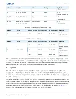
A 4-layer PCB layout is recommended to be used for all GR551x package options.
layer stackup (thickness: 1.6 mm) of GR551x.
Figure 3-6 GR551x PCB layer stackup
L1: top layer where components, RF transmission lines, and key signal lines are placed
L2: internal ground plane layer, used for both the ground return path and the reference plane for the 50 ohm RF
transmission line
L3: internal routing layer, used to split power domains and place a small number of signal lines
L4: bottom layer where components and signal lines are placed
Note
:
The customer’s product design can be adjusted according to the actual situation. Two typical examples for designing 4-
layer PCB layouts are provided in “
Section 4.2.1 Four-layer PCBs in QFN56 Package
”, to help users quickly get started with development and PCB layout design.
For users who need to reduce costs on QFN packages, they shall choose 2-layer PCBs, with special attention to the
layout of power filter components, power input, the ground return path for DC-DC buck converters, and completeness
of the reference plane for RF route. For details on the layout and routing, see “
Section 4.2.2 Two-layer PCBs in QFN
”.
3.2.2 Components Layout
All components operating at high frequency should have their layout made as compact as possible. This will prevent
the cross-coupling between lines and also minimize the parasitic effects which will have a negative impact on the
operating parameters.
Copyright © 2021 Shenzhen Goodix Technology Co., Ltd.
32


