background image

Cinterion

® 

LGA DevKit User Guide

4 LGA DevKit Interfaces

27

lga_devkit_ug_v02

2019-05-27

Preliminary

Page 9 of 28

4

LGA DevKit Interfaces

4.1

USB

The LGA DevKit comes with two USB interfaces supporting power supply and serial commu-
nication. You may choose to setup communication via a module's USB port and/or a module's
UART (ASC0) port via FTDI232R VCP.

Both USB ports can be used in parallel while power is sourced from both ports.

The native USB power is isolated from the VCP USB power by a diode, meaning that the
VCP USB power does not feedback to the native USB power, but vice versa. This should
be taken into account when supplying the LGA DevKit from different USB power sources,
depending on the voltage levels there could be a power feedback from native USB to VCP
USB.

In case of marginal USB power supply both USB ports should be used to improve power
capabilities.

Note:

 The modem's USB driver can be downloaded from the LGA DevKit's web page that can

be reached by scanning the QR code.

4.2

SIM

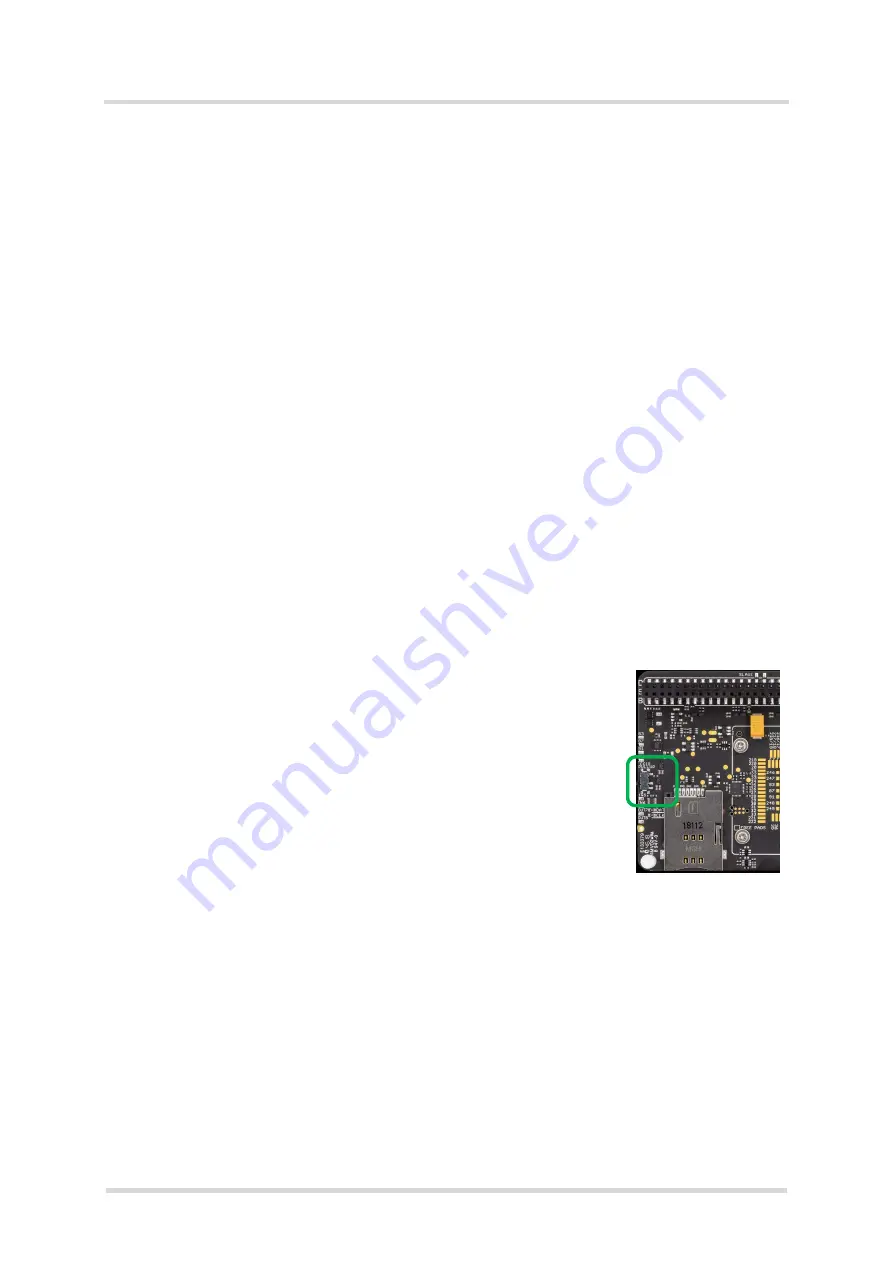
On the LGA DevKit's bottom side you find a SIM card holder that is
connected to the module's regular SIM interface lines, except for the
CCIN line where the (default) jumper needs to be set for CCIN at the
CONTROL pin headers (see 

Section 4.3

). However, some modules

come with an additional SIM interface. This can be accessed in con-
junction with a DSB75/DSB-Mini (as port extender) to support dual
SIMs - with the DSB75/DSB-Mini serving as the second SIM interface. 

Some Cinterion

®

 modules require additional components at the SIM

interface, for instance pull-up resistors managed by the DevKit's con-
trol logic. These can be overridden by setting a switch on the DevKit's
bottom side - see 

Figure 4

. For modules requiring a CCIO pull up re-

sistor this switch should be set to "CCIO PULLUP" (see 

Section 7.3

). 

Figure 4:  

SIM settings

Summary of Contents for Cinterion LGA DevKit

Page 1: ... GEMALTO COM M2M Cinterion LGA DevKit User Guide Version 02 DocId lga_devkit_ug_v02 ...

Page 2: ...GHT TO USE THE DOCUMENT THE RECIPIENT SHALL NOT COPY MODIFY DISCLOSE OR REPRODUCE THE DOCUMENT EXCEPT AS SPECIFI CALLY AUTHORIZED BY GEMALTO M2M Copyright 2019 Gemalto M2M GmbH a Thales Company Gemalto the Gemalto logo are trademarks and service marks of Gemalto and are registered in certain countries Microsoft and Windows are either registered trademarks or trademarks of Microsoft Corporation in ...

Page 3: ...ace Selection 11 4 7 PWR Switch Power Source Selection 11 4 8 Free Level Shifters 12 4 9 LEDs 12 4 10 Patch Field 12 4 11 RF Antenna 13 4 12 Power Supply 14 4 12 1 Supply Current Measurement 14 4 12 2 External Reference Supply 15 5 General Characteristics 16 5 1 Limits 16 5 2 Electrical Properties 16 6 Operating DevKit on DSB75 and DSB Mini 17 6 1 Quick Start Operating LGA DevKit and DSB75 17 7 Mo...

Page 4: ...Cinterion LGA DevKit User Guide Contents 28 lga_devkit_ug_v02 2019 05 27 Preliminary Page 4 of 28 9 Package Content 21 10 Appendix 22 10 1 Placement 22 10 2 Schematics 23 10 3 Errata Troubleshooting 26 ...

Page 5: ...tform modules Either one of the LGA DevKit variant SM or L needs to be ordered together with the LGA DevKit Socket leaving the option to reuse the Socket for the other LGA DevKit variant 1 1 Feature and Benefits LGA DevKit Socket supports four different module footprints for industrial industrial plus modules With LGA DevKit SM LGA106 LGA114 and LGA120 With LGA DevKit L LGA156 Future proof ready f...

Page 6: ...R LED may indicate issues that should be corrected For de tails see Section 4 9 Note By scanning the QR code at the back of the LGA DevKit you will also find further information videos and available drivers 2 1 Mounting the LGA DevKit Socket Before operating the socket has to be mounted onto the LGA DevKit with 4 screws Scanning the QR code on the DevKit s back and or the quick start guide will le...

Page 7: ...ion LGA DevKit User Guide 3 LGA DevKit Overview 27 lga_devkit_ug_v02 2019 05 27 Preliminary Page 7 of 28 3 LGA DevKit Overview 3 1 Top and Bottom View Figure 1 LGA DevKit top view Figure 2 LGA DevKit top view ...

Page 8: ...Industrial Multifootprint Power 80Pin DSB75 DSB Mini Connector ASC0 Micro USB NativeMicro USB RF Main DRX Antenna Connector On board Sim Connector Combinded Powering MCU control unit Error detection LED Footprint detection Button ON BTN Button RST BTN USB Data Module Signals Power SIM Antenna ASC0 Signal Module Signals StatusLEDS Power User Interface Connectors Power Block Logical Block Controllin...

Page 9: ...supply both USB ports should be used to improve power capabilities Note The modem s USB driver can be downloaded from the LGA DevKit s web page that can be reached by scanning the QR code 4 2 SIM On the LGA DevKit s bottom side you find a SIM card holder that is connected to the module s regular SIM interface lines except for the CCIN line where the default jumper needs to be set for CCIN at the C...

Page 10: ...s the right side corresponds to peripherals like level shifters or the DSB connector green box in Figure 5 Placing a jumper connects a line through a level shifter to the associated pin at the 2x40 pin connector at the bottom of the LGA DevKit and thus to a connected DSB75 DSB Mini See also Figure 3 Not placing a jumper leaves a module signal line open External periphery can also be connected to a...

Page 11: ...le Please note that this functionality is only available if the default jumper is set for EMERG_RST at the CONTROL pin headers see Section 4 3 4 6 ASC0 Switch Module UART Interface Selection The ASC0 switch selects the module s UART communication interface either via USB VCP FTDI232R or via RS232 D Sub interface on the DSB75 DSB Mini Changing this from USB to RS232 during operation resets the FTDI...

Page 12: ...ifters are accessible close to the patch field as well with the reference Vext and Vref The Vref related lev el shifter connections can also be accessed via four addi tional pads at the left bottom side of the LGA DevKit where additional pins may be soldered Attention You will lose your warranty if the patch field was soldered used Figure 7 Patch field RED Blinking continuously Module is inserted ...

Page 13: ...N and DRX can used for radio transmission The GNSS interface is supported by an U FL connector named GPS All antenna interfaces have additional ESD protection implemented Figure 8 S11 MAIN antenna module RF pad and S21 MAIN antenna RF loss The LGA DevKit package includes a broad band high efficiency PCB antenna that can be used with the DevKit for all radio band combinations Figure 9 Antenna S11 ...

Page 14: ...the power has been reset As a recommendation the LGA DevKit should be supplied with 5V 1A over one or two USB ports The onboard bypass capacitors should buffer enough energy to support short 2G peak currents up to 2 5A 4 12 1 Supply Current Measurement The LGA DevKit supports three methods to measure the current consumption of the inserted module Measure the voltage across the on board 100 mOhm sh...

Page 15: ...ternal reference voltage may be connected By default i e without an external reference voltage connected the interface operates at 3V to meet the DSB75 DSB Mini requirements But if it is required to operate the interface at another voltage an external source in the range between 1 2V 5V can be connected to REF IN and GND as shown in Figure 11 Figure 11 External reference supply and pin header for ...

Page 16: ...te maximum ratings Parameter Min Max Unit Voltage on USB ports 0 3 5 5 V Voltage on DSB port 0 3 5 5 V Voltage on signal pin header depending on used module 0 3 2 1 V Current signal pin header depending on used module 10 10 mA Voltage on external reference 0 3 6 V Socket single contact continues current 2 A Table 2 Operating conditions Parameter Min Max Unit Recommended operating condition Supply ...

Page 17: ... select the first UART If you select RS232 the modules ASC0 is conducted to the DSB and can be accessed on the D SUB connector If you select USB the UART can be accessed via USB VCP port Note that the USB VCP bridge will be in reset state while RS232 is activated As a conse quence the interface is de enumerated on host side Please refer to Section 10 3 for a DSB Mini patch needed to operate ASC0 o...

Page 18: ...t Therefore please connect IO25 and VEXT via a jumper 7 2 EHS5 6 8 Operation Some early samples of EHS5 6 8 require the AUTO_ON circuit For these samples please con nect A_ON to GND or else the module will not start 7 3 EMS31 Operation EMS31 V requires a pull up resistor for the SIM interface Please use the SIM switch setting mentioned in Section 4 2 7 4 ENS22 Operation With ENS22 the white ON LED...

Page 19: ...New document Cinterion LGA DevKit User Guide v02 New document Cinterion LGA DevKit User Guide v01 8 2 Related Documents 1 Hardware Interface Description for your Gemalto M2M module 2 AT Command Set for your Gemalto M2M module To visit the Gemalto M2M website you can use the following link http www gemalto com m2m Chapter What is new Throughout document Revised document Chapter What is new Initial ...

Page 20: ...LGA DevKit is intended for evaluation and development purposes only and should therefore only be used in a laboratory test environment The device is not CE ap proved and has not been authorized as required by the rules of the FCC All persons handling the Cinterion LGA DevKit must be properly trained in electronics and observe good engineer ing practice standards Pacemaker patients are advised to k...

Page 21: ...0 Base PCB for the industrial platform modules USB and SMA cable An ultra wideband high efficiency antenna A bag of jumpers 25pcs A quick start guide Cinterion LGA DevKit L Ordering number L30960 N0112 A100 Base PCB for the industrial plus platform modules USB and SMA cable An ultra wideband high efficiency antenna A bag of jumpers 25pcs A quick start guide Cinterion LGA DevKit Socket SM L Orderin...

Page 22: ...2 C53 C57 C58 C59 C60 C61 C62 C63 C64 C65 C66 C67 C68 C69 C70 C71 C72 C73 C74 C75 C76 C77 C78 CON8 D1 D2 D3 D5 IC1 IC2 IC3 IC4 IC5 IC6 IC 7 IC8 IC9 IC10 IC11 IC14 IC15 IC16 IC17 IC18 IC19 IC20 IC21 IC22 IC99 JP1 JP7 L28 L29 L30 L31 L32 L33L34 L35 LED7 R1 R2 R3 R4 R5 R6 R7 R8 R9 R10 R11 R12 R13 R14 R15 R16 R17 R18 R19 R20 R21 R22 R23 R24 R25 R27 R28 R29 R30 R31 R32 R33 R34 R35 R36 R37 R38 R39 R40 R...

Page 23: ...0_D4 2 GND VCC 4 3 IC9B GND VCC 18 16 IC9C R87 R88 TP57 TP61 R96 S1 A B R97 T15B R98 TP66 TP75 TP77 TP78 TP79 TP80 VOUT 5 VIN 1 EN 3 GND 2 BP 4 IC11 C75 C76 C77 C78 R99 LED9 R100 R101 D5 R103 CON2 GND GND CON3 GND GND TP4 TP5 TP6 TP10 T17A 5 3 4 T15A GND 2 GND 2 GND 2 ANT_GPS ANT_GPS AGND 3 AGND 3 VMIC 3 VMIC 3 MICN1 3 MICN1 3 EPP1 3 EPP1 3 EPN1 3 EPN1 3 MICP1 3 MICP1 3 I2CCLK 2 I2CCLK 2 I2CDAT 2 ...

Page 24: ...T5B 2 6 1 3 1 5 4 2 T10 T14A T14B R26 T11B T11A JP2 1 2 3 4 5 6 7 8 9 10 FLT 6 DVDT 1 EN UVLO 2 GND 8 2 ILM 7 IN 3 2 OUT 5 T6 3 1 5 4 2 T16 3 1 5 4 2 C57 R57 LED6 R63 IC10 IN 9 2 EN 7 GND 5 2 OUT 1 2 FB 3 SS 6 PB 4 R75 5 3 4 T1A 2 6 1 T1B R76 R77 R78 R79 R80 R81 C73 C74 D2 D1 R84 R85 CON17 P 1 P 2 P 3 P 4 P 5 P 10 P 6 2 P 8 2 P 11 CON18 P 1 P 2 P 3 P 4 P 5 P 10 P 6 2 P 8 2 P 11 R60 R86 R90 R91 R92...

Page 25: ...2 3 B2 6 VCC A 1 VCC B 8 GND 4 C59 C61 C62 C63 C64 C65 C66 JP6 1 2 3 4 5 6 7 8 9 10 11 12 JP7 1 2 3 4 SCL 1 VSS 2 SDA 3 VCC 4 NC 5 TP52 TP53 TP54 TP55 C67 C68 C69 C70 C71 R82 C72 T3A R83 TP59 TP60 T3B R89 TP11 TP12 TP16 TP17 TP18 TP73 TP74 TP82 TP83 D4 RTS0_X100 2 RTS0_X100 2 CTS0_X100 2 CTS0_X100 2 DTR0_X100 2 DTR0_X100 2 DSR0_X100 2 DSR0_X100 2 DCD0_X100 2 DCD0_X100 2 TXD0_X100 2 TXD0_X100 2 RXD...

Page 26: ... RF path loss right of the PCB s B22 revision Radio Temperature Measurement The LGA DevKit comes with minor limitations in terms of radio frequency and temperature eval uation because of a slightly increased RF path loss and module temperature encapsulation in side the LGA socket PCB22 23 with DSB Mini as Expander Board ON LED When the DSB Mini is used as port expander there is a current back feed...

Page 27: ...ules with bold lettering QUALCOMM e g EXS81 or wrongly positioned RohS sym bol e g ELS61 81 on the module s bottom side might be detected as a wrong footprint and will therefore not be powered up This limitation will be fixed in an upcoming version PCB B22 Error LED TXD0 LED The LGA DevKit s PCB revision B22 has a softly glowing error LED Also when no module is inserted the TXD0 LED glows softly T...

Page 28: ...entity modules security solutions and licensing and monetization solutions to streamline development timelines and provide cost efficiencies that improve the bottom line As an experienced software provider we help customers manage connectivity security and quality of service for the long lifecycle of IoT solutions For more information please visit www gemalto com m2m www facebook com gemalto or Fo...

Reviews: