background image

Change even page title here 

Chapter 3 Jumpers and Switches 

FMEMCU-UG-960031-13 

- 24 - 

© Fujitsu Semiconductor Europe GmbH 

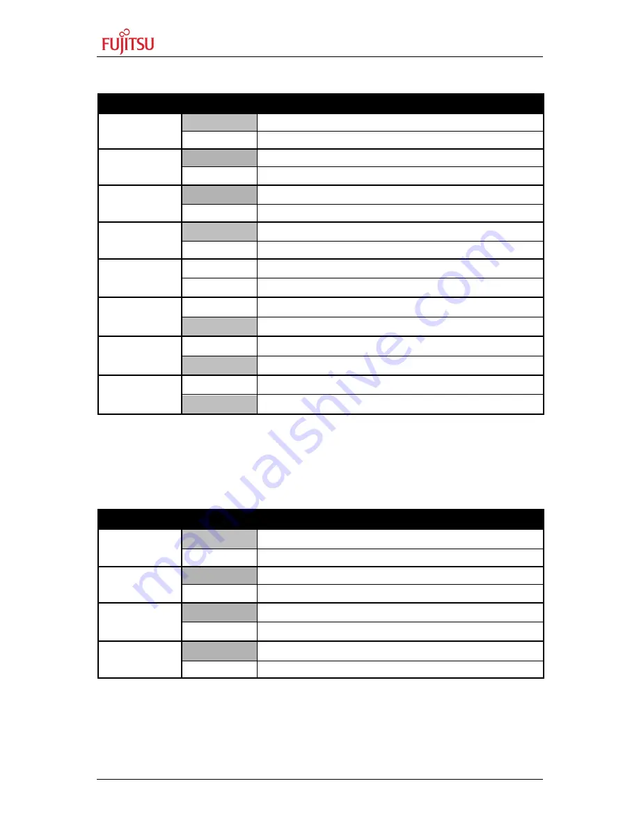
3.10.2 LIN-UART 2 (JP: 36, 37, 38, 39, 40, 42, 43, 45) 

Jumper 

Setting 

Description 

JP37 

(RXD) 

1-2 

SIN2 is connected to RS232 transceiver 

2-3 

SIN2 is connected to LIN transceiver


JP39 

(TXD) 

1-2 

SOT2 is connected to RS232 transceiver 

2-3 

SOT2 is connected to LIN transceiver


JP40 

(RS232/LIN) 

1-2 

X9 pin 2 is connected to RS232 transceiver 

2-3 

X9 pin 2 is connected to LIN transceiver 

JP36 

(RTS-CTS) 

Closed 

RTS and CTS of X9 are connected 

Open 

RTS and CTS of X9 are not connected 

JP38 

(DTR/RTS) 

1-2 

DTR signal (pin 6 of X9) is used as reset source 

2-3 

RTS signal (pin 7 of X9) is used as reset source


JP43 

(LIN enable) 

Closed 

LIN transceiver for X5 is enabled 

Open 

LIN transceiver for X5 is disabled 

JP45 

(LIN master) 

Closed 

LIN-UART2 is LIN Master 

Open 

LIN-UART2 is LIN Slave 

JP42 

(LIN Vbat) 

Closed 

LIN bus (X9 pin 1) is powered by the board 

Open 

LIN bus (X9 pin 1) is not powered by the board 

Table 3-10: UART2 Settings 


3.11  CAN interfaces 

(JP: 24, 26, 34, 35)


Two high-speed CAN-

transceivers can be connected to the microcontroller‟s CAN interfaces 

(CAN0 and CAN1). 

Jumper 

Setting 

Description 

JP24 

(CAN0 RX) 

Closed 

RX0 is connected to CAN0 (X6) 

Open 

RX0 is disconnected to CAN0 (X6)


JP26 

(CAN0 TX) 

Closed 

TX0 is connected to CAN0 (X6) 

Open 

TX0 is disconnected to CAN0 (X6)


JP34 

(CAN1 RX) 

Closed 

RX1 is connected to CAN1 (X8) 

Open 

RX1 is disconnected to CAN1 (X8) 

JP35 

(CAN1 TX) 

Closed 

TX1 is connected to CAN1 (X8) 

Open 

TX1 is disconnected to CAN1 (X8) 

Table 3-11: CAN Settings 


Summary of Contents for SK-96650_6A0_380-120PMC

Page 1: ...Fujitsu Semiconductor Europe User Guide FMEMCU UG 960031 13 F MC 16FX FAMILY MB96650 6A0 6C0 380 SERIES EVALUATION BOARD SK 96650_6A0_380 120PMC USER GUIDE ...

Page 2: ...ductor Europe GmbH Revision History Date Issue 13 04 2011 V1 0 SWi First Release 06 06 2011 V1 1 Swi JP47 added in description Chapter 2 3 title changed 02 03 2011 V1 2 SWi name convention 24 04 2012 V1 3 SWi new chapter about CE conformity declaration This document contains 39 pages ...

Page 3: ...placement of the hardware deliverable or parts thereof if the deliverable is returned to FSEU in original packing and without further defects resulting from the customer s use or the transport However this warranty is excluded if the defect has resulted from an accident not attributable to FSEU or abuse or misapplication attributable to the customer or any other third party not relating to FSEU or...

Page 4: ...us 9 1 3 9 Emulator System 9 1 3 10 On Chip Debug System OCDS 9 2 INSTALLATION 10 2 1 Connection Power On 10 2 2 Default Jumper Settings 11 2 3 Jumper Location 13 2 3 1 MB96650 13 2 3 2 MB966A0 6C0 14 2 3 3 MB96380 15 3 JUMPERS AND SWITCHES 16 3 1 P17_0 JP51 16 3 2 Operating Mode S1 16 3 3 Power Supply S2 JP 8 15 16 17 22 61 62 63 64 17 3 4 Subclock JP 1 2 19 3 5 Analog Power Supply Voltage JP 11 ...

Page 5: ... In Circuit Programming Connector X4 29 4 7 Debug Connector X12 29 4 8 Alarm Comparator Connector J2 29 4 9 External Supply Voltage Vin J3 29 4 10 Vcc 5 Volts J4 30 4 11 Vcc 3 3 Volts J5 30 4 12 LIN Bus Inhibit J6 30 4 13 LIN Bus Inhibit J11 30 4 14 VCC Connector J7 30 4 15 GND Connector J8 30 5 PROGRAMMING THE INTERNAL FLASH MEMORY 31 5 1 Asynchronous Mode 31 5 1 1 Reset optional 32 5 1 2 Flash P...

Page 6: ...rd for the Fujitsu MB96600 Flash microcontroller MB96650 MB966A0 and MB966C0 Series as well as for the MB96300 Flash microcontroller MB96380 Series It can be used stand alone for software development and testing or as a simple target board to work with the emulator system The board allows the designer immediately to start software development before his own final target system is available ...

Page 7: ...er supply On board 3 3V and 5 0V switching mode voltage regulators Power LEDs for all supply voltages Onboard voltage supervisor monitor In Circuit serial Flash programming UART0 or UART2 All resources available for evaluation All MCU pins routed to connectors 4 MHz main crystal 32 kHz crystal for sub clock operation Two RS232 or LIN interfaces Two CAN interfaces 3 V capable CAN LIN and RS232 tran...

Page 8: ... All transceivers are fully 3 3V IO compatible to enable low voltage applications In circuit programming asynchronous can be done via LIN UART 0 and 2 X5 X9 1 3 3 CAN Bus Two high speed CAN transceivers TLE6250GV33 can be connected to the CAN interfaces of the MCU to allow easy connection to CAN networks All transceivers are fully 3 3V IO compatible to enable low voltage applications 1 3 4 MCU Pin...

Page 9: ... is used as an emulator target board for the MB96300 super series the microcontroller must be removed from the socket and the corresponding probe cable has to be mounted Table 1 1 Emulation System 1 3 10 On Chip Debug System OCDS If the On Chip debugging on the MB96600 microcontroller is applied then the embedded emulator MB2100 01 E must be connected to the target board via SMA jack on the PCB Se...

Page 10: ...s Do not use any other probe cable than MB2198 16FX 120P M21 only Connect the probe cable to the MB2198 500 E emulation Adapter Board Check all jumper settings of the evaluation board the Probe Cable and the Adapter Board When turning on the system be sure to use the following power up sequence 1 Power up the Emulator Main Unit MB2198 01 2 Power up the Adapter Board MB2198 500 if needed 3 Power up...

Page 11: ... 1 2 1 2 D 4 JP21 SIN0 RS232 LIN transceiver Jumper 3 pin 1 2 1 2 1 2 H 5 JP22 Mains Switch Jumper 2 pin Open Open Open L 16 JP23 UART0 DTR RTS Jumper 3 pin Open Open Open H 3 JP24 CAN0 RxD Jumper 2 pin Closed Closed Closed D 4 JP25 SOT0 RS232 LIN transceiver Jumper 3 pin 1 2 1 2 1 2 H 5 JP26 CAN0 TxD Jumper 2 pin Closed Closed Closed D 3 JP27 UART0 RS232 LIN Jumper 3 pin 1 2 1 2 1 2 I 3 JP28 UART...

Page 12: ...efault Setting Coordinates MB96650 MB966A0 MB966C0 MB96380 JP61 DVCC Pin 53 Jumper 2 pin Open Closed Closed K11 JP62 DVSS Pin 54 Jumper 2 pin Open Open Closed K11 JP63 DVCC Pin 41 Jumper 2 pin Open Open Closed K12 JP64 DVSS Pin 42 Jumper 2 pin Open Closed Closed K12 JP78 ALARM0 Jumper 2 pin Closed Closed Closed L 13 Table 2 1 Jumper Settings ...

Page 13: ...ng figures show the silk plot of the starter kit with marked default jumper settings depending on the microcontroller series 2 3 1 MB96650 A B C D E F G H I J K L M 1 1 2 2 3 3 4 4 5 5 6 6 7 7 8 8 9 9 10 10 11 11 12 12 13 13 14 14 15 15 16 16 17 17 18 18 19 19 20 A B C D E F G H I J K L M 20 Figure 2 1 Default Jumper Setting with MB96650 ...

Page 14: ...031 13 14 Fujitsu Semiconductor Europe GmbH 2 3 2 MB966A0 6C0 A B C D E F G H I J K L M 1 1 2 2 3 3 4 4 5 5 6 6 7 7 8 8 9 9 10 10 11 11 12 12 13 13 14 14 15 15 16 16 17 17 18 18 19 19 20 A B C D E F G H I J K L M 20 Figure 2 2 Default Jumper Setting with MB966A0 6C0 ...

Page 15: ...miconductor Europe GmbH 15 FMEMCU UG 960031 13 2 3 3 MB96380 A B C D E F G H I J K L M 1 1 2 2 3 3 4 4 5 5 6 6 7 7 8 8 9 9 10 10 11 11 12 12 13 13 14 14 15 15 16 16 17 17 18 18 19 19 20 A B C D E F G H I J K L M 20 Figure 2 3 Default Jumper Setting with MB96380 ...

Page 16: ...ch is closed JP50 Connects DIP switch to temporary mode pin P17_0 MB96300 MD1 Jumper Setting Description MB96650 MB966A0 MB966C0 MB96380 JP51 P17_0 Closed Closed Closed Pin 63 connected to DIP Switch S1 Open Open Open Pin 63 disconnected to DIP Switch S1 Table 3 1 P17_0 Jumper Configuration 3 2 Operating Mode S1 This switch controls the MCU operation mode after Reset Please take care of the follow...

Page 17: ... suitable for the connected bus devices mostly around 12V Since there is a protection diode between Vin and Vs it is not possible to power the board over the LIN bus S2 Power Switch JP8 Core power supply stabilization capacitor JP15 Selects the power supply voltage for the microcontroller JP16 Connects the power supply voltage to the microcontroller An ampere meter can be used instead for power co...

Page 18: ...voltage is set to 3 3V JP22 Mains Closed Closed Closed Board is always switched on Open Open Open Board power is controlled by switch S2 JP61 DVCC_53 Closed Closed Closed Pin 53 is connected to SMC DVCC supply voltage Open Open Open Pin 53 is disconnected to SMC DVCC supply voltage JP62 DVSS_54 Closed Closed Closed Pin 54 is connected to SMC DVSS supply voltage Open Open Open Pin 54 is disconnecte...

Page 19: ...0 P04_1 instead Please check the related datasheet JP1 defines usage of pin 69 X1A JP2 defines usage of pin 68 X0A Jumper Setting Description JP2 X0A 1 4 Pin 68 is connected to the 32 kHz sub clock X0A 2 4 Pin 68 is used as port pin P04_0 3 4 Pin 68 is connected to GND in case that subclock device is used but no 32 kHz crystal is connected JP1 X1A 1 2 Pin 69 is connected to the 32 kHz sub clock X1...

Page 20: ... disconnected from GND 1 By default the resistor network R16 R17 R20 R21 is not mounted on the board Table 3 5 ADC Supply Default JP11 JP12 JP13 and JP14 are closed By default the A D converter supply and reference voltage is the same as the microcontroller supply voltage Note If JP11 and JP14 are open the user has to supply an adequate analog voltage supply AVcc and AVss to the A D converter If J...

Page 21: ...3 UART RESET 1 2 X5 UART0 is used to generate Reset 2 3 X9 UART2 is used to generate Reset Open No UART is used to generate Reset JP41 DTR DTRx 1 2 No polarity inversion for the DTR RTS signal 2 3 Polarity inversion for the DTR RTS signal JP46 Reset imm delayed 1 2 Reset is applied immediately when SW6 is pressed 2 3 Reset is applied when SW6 is pressed 2sec JP48 RST MCU Closed External reset gene...

Page 22: ...o SW3 Open No connection to the microcontroller JP6 SW4 Closed Pin 18 IN0 TTG4 0 of the MCU is connected to SW4 Open No connection to the microcontroller JP7 SW5 Closed Pin 19 IN1 TTG5 1 of the MCU is connected to SW5 Open No connection to the microcontroller Table 3 8 User Push Buttons Default JP3 4 5 6 7 closed By default all push buttons are connected to the microcontroller 3 9 I2 C pull up res...

Page 23: ... Description JP21 RXD 1 2 SIN0 is connected to RS232 transceiver 2 3 SIN0 is connected to LIN transceiver JP25 TXD 1 2 SOT0 is connected to RS232 transceiver 2 3 SOT0 is connected to LIN transceiver JP27 RS232 LIN 1 2 X5 pin 2 is connected to RS232 transceiver 2 3 X5 pin 2 is connected to LIN transceiver JP19 RTS CTS Closed RTS and CTS of X5 are connected Open RTS and CTS of X5 are not connected J...

Page 24: ... X9 is used as reset source JP43 LIN enable Closed LIN transceiver for X5 is enabled Open LIN transceiver for X5 is disabled JP45 LIN master Closed LIN UART2 is LIN Master Open LIN UART2 is LIN Slave JP42 LIN Vbat Closed LIN bus X9 pin 1 is powered by the board Open LIN bus X9 pin 1 is not powered by the board Table 3 10 UART2 Settings 3 11 CAN interfaces JP 24 26 34 35 Two high speed CAN transcei...

Page 25: ...d Monitor Voltage JP24 As the 3rd sense input of the triple power supply monitor iC U12 is as reset detection it is recommended to connect this input to 3 3V Jumper Setting Description JP24 Monitor 1 2 iC monitor input connected to 1 8V forbidden 2 3 iC monitor input connected to 2 5V 2 4 iC monitor input connected to 3 3V ...

Page 26: ... and so on 4 3 LIN UART connectors X5 X9 Two 9 pin D Sub female connectors are used for the serial interfaces Note that X5 and X9 are shared between the RS232 and LIN transceivers and must be configured to the desired functionality refer to chapter 3 10 for details Figure 4 2 UART Connector Pin Number Pin Signal Description 1 VBat Power from to LIN bus 2 TXD RS 232 transmit output LIN Bi direction...

Page 27: ...or the CAN interfaces CAN0 and CAN1 Both CAN interfaces can be used simultaneously Figure 4 3 CAN Connector Pin Number Pin Signal Description 1 NC Not used 2 CANL LOW level CAN voltage input output 3 GND Ground 4 NC Not used 5 NC Not used 6 NC Not used 7 CANH HIGH level CAN voltage input output 8 NC Not used 9 NC Not used Shield GND Ground Table 4 2 CAN Connector Signals ...

Page 28: ...1 can be used to adjust the contrast of the LC Display Pin 15 and 16 of J1 are normally not mounted If the used LC Display has pins for LED backlight at this position they can be connected here Pin15 Vcc via 39Ω 0 5W Pin16 GND The contrast of an optional LC Display connected to J1 can be adjusted by RP1 The following control signals are provided Figure 4 4 User LEDs LCD 15 1 16 1 2 3 4 5 6 7 8 9 1...

Page 29: ...STX MCU reset signal 6 SIN2 UART2 receive data 7 SOT2 UART2 transmit data 8 SCK2 UART2 clock 9 VCC Board supply voltage 10 GND Ground Table 4 4 In circuit programming connector 4 7 Debug Connector X12 The MB96600 microcontroller series facilitates on chip debugging via a single wire system with the embedded emulator MB2100 01 E The emulator is connected to the starter kit via SMA jack Figure 4 6 D...

Page 30: ... 3 3 Volts J5 On this connector the VCC3V3 supply can be measured 4 12 LIN Bus Inhibit J6 To this connector the INH pin of the LIN0 transceiver is connected 4 13 LIN Bus Inhibit J11 To this connector the INH pin of the LIN1 transceiver is connected 4 14 VCC Connector J7 On this connector the VCC supply see chapter 3 3 can be measured 4 15 GND Connector J8 Ground reference terminal GND ...

Page 31: ... connectors X5 or X9 which are connected to UART0 and UART2 respectively can be used on the starter kit The following jumper settings are necessary Jumper Programming UART Setting Description JP21 SIN0 UART0 1 2 SIN0 is connected to RxD of X5 JP25 SOT0 UART0 1 2 SOT0 is connected to TxD of X5 JP27 RS232 LIN UART0 1 2 RS232 transceiver is selected for X5 JP28 Vbat UART0 Open X5 1 is disconnected fr...

Page 32: ... A B UART0 or UART2 1 2 LIN UART 0 X5 is used to generate reset 2 3 LIN UART 2 X9 is used to generate reset JP41 DTR DTRx UART0 or UART2 1 2 No negation for the DTR RTS signal 2 3 DTR RTS signal is negated Table 5 3 Jumper Settings for reset signal 5 1 2 Flash Programming 1 Configure the microcontroller mode Note JP51 don t care Note JP51 closed Connect the configured UART see above to your serial...

Page 33: ...sly special third party soft and hardware has to be used e g GALEP 4 from www conitec de This tool is not available for free A dedicated Flash programming socket X4 is provided on the evaluation board for direct connection to this programmer X4 Flash programming socket Figure 5 1 Flash Programming Socket Note Please open the jumpers JP37 SIN2 and JP39 SOT2 in order to avoid that the synchronous pr...

Page 34: ... 6 On Chip Debug Hardware Configuration With the MB9600 series on chip debugging is possible In case of the usage following hardware configuration on the starter kit has to be done JP51 don t care Set DIP switch X12 into run mode On Off 1 2 3 4 DEBUG I F P17_0 MD nc DIP Switch RUN Mode On Off 1 2 3 4 MD0 MD1 MD2 nc MB96600 MB96300 ...

Page 35: ... header for package FPT 120P M21 LQFP 120 Tokyo Eletech Corp http www tetc co jp e_index htm MB2100 01 E Embedded emulator for MB96600 Series MB2198 01 E Emulator debugger main unit MB2198 500 E Emulation Pod of MB2198 01 MB2198 16FX 120P M21 Emulator probe cable for MB96F38x MCU MB96300 Series MB96V300 MB96300 Series Evaluation chip MB96F38xRS Flash MCU Single Clock MB96F38xRS Flash MCU Dual Cloc...

Page 36: ...OR Products can be found on the following Internet pages Microcontrollers 8 16 and 32bit Graphics Controllers Datasheets and Hardware Manuals Support Tools Hard and Software http mcu emea fujitsu com Power Management Products http www fujitsu com emea services microelectronics powerman index html For more information about FUJITSU SEMICONDUCTOR http emea fujitsu com semiconductor ...

Page 37: ...hre Gültigkeit We Fujitsu Semiconductor Europe GmbH Pittlerstrasse 47 63225 Langen Germany hereby declare that the design construction and description circulated by us of this board complies with the appropriate basic requirements according to the EU Guideline 2004 108 EC entitled Electro Magnetic Compatibility Any changes to the equipment hardware and or software will render this declaration inva...

Page 38: ...Change even page title here Chapter 10 China RoHS regulation FMEMCU UG 960031 13 38 Fujitsu Semiconductor Europe GmbH 10 China RoHS regulation This board is compliant with China RoHS ...

Page 39: ...r zurück Zur Entsorgung schicken Sie das Gerät bitte an die folgende Adresse Fujitsu SEMICONDUCTOR Europe GmbH Warehouse Disposal Monzastraße 4a D 63225 Langen Valid for European Union Countries According to the European WEEE Directive and its implementation into national laws we take this device back For disposal please send the device to the following address Fujitsu SEMICONDUCTOR Europe GmbH Wa...

Reviews: