


MPC563XM Reference Manual, Rev. 1
Freescale Semiconductor
841
Preliminary—Subject to Change Without Notice
first filter clock period in which the signal is continuously stable. This may add to the latency and also to
the minimum detected signal pulse in a noisy environment.
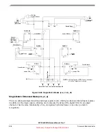
23.4.5.6.4
Filter Clock Prescaler
The TCRCLK signal and each channel configured as an input have an associated synchronizer followed
by a digital filter connected to the signal that samples signal transitions. After reset, the digital filter filters
out high and low pulse widths smaller than the period of two system clocks with FCSS=0, or 1 system
clock with FCSS=1, preventing these transitions from being input to the transition detect logic. For
FPSCK=0 and FCSS=0, the synchronizer and digital filter are guaranteed to pass pulses that are as wide
as or wider than four system clocks, meaning a minimum period of 8 system clocks. These figures are
halved by setting FCSS=1.. By changing the FPSCK field in register ETPUECR the user can select a lower
clock rate for the filter signal to define wider valid pulses and filter out wider noise pulses. The filter
prescaler clock control is a division of the system clock. To guarantee pulse detection by the digital filter,
the pulse must cover at least the stated number of samples at the filter clock rate. For example, a two
sample digital filter must sample two points in the pulse to detect it.
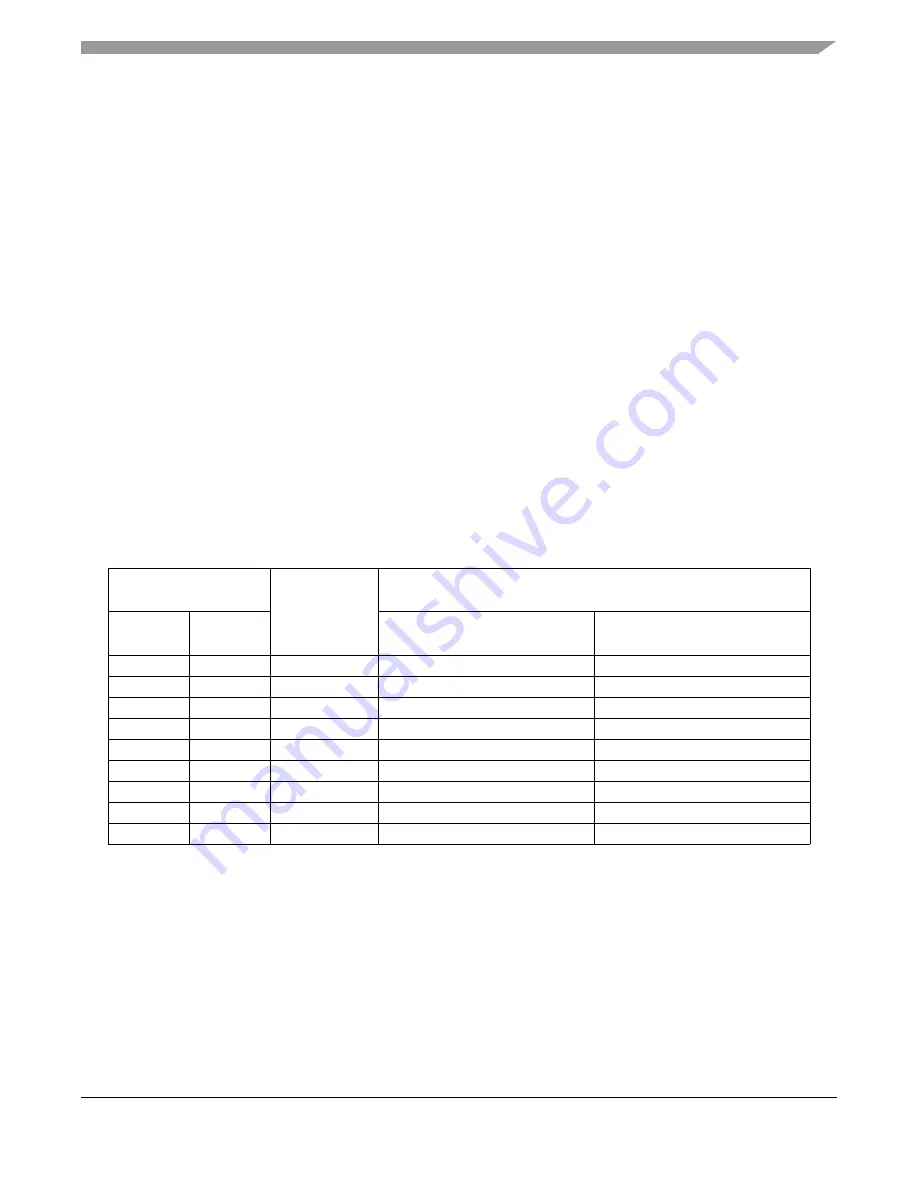
guaranteed detected pulse width and the maximum filtered noise pulse width. The table refers only to the
digital filter operation. The external un-synchronized pulses must be wider by two extra system clocks to
ensure detection through both the synchronizer and the digital filter. Delays introduced by synchronizer,
filter and edge detection logic are explained in
Section 23.6.1.2, “Input/Output Signal Delays
NOTE
If the ETPUTBCR field TCRCF selects the filter clock of the channels (see
Section 23.3.3.1, “ETPUTBCR - eTPU Time Base Configuration Register
),
the TCRCLK filter will be clocked as if FCSS=0. always dividing system
clock /2 using FPSCK, regardless if FCSS is 0 or 1.
Table 23-38. Pulse Widths and Delays
Filter Control
(FPSCK)
Sample on
System Clock
Divided by:
Min. Width Guaranteed Detected / Max. Width filtered
(Min. Filter Delay / Max. Filter Delay)
1
1
This table shows pulse widths in number of periods of the system clock.
FCSS = 0
FCSS = 1
Two-Sample or Continuous
Mode
Three-Sample or Integrator
2
Mode
2
Integrator mode is available for TCRCLK filtering only, see
Section 23.4.6.5, “TCRCLK Digital Filter
.”
not avail.
000
1
2 / 1 (2 / 3)
3 / 2 (3 / 4)
000
001
2
4 / 2 (3 / 3)
6 / 4 (5 / 5)
001
010
4
8 / 4 (5 / 7)
12 / 8 (9 / 11)
010
011
8
16 / 8 (9 / 15)
24 / 16 (17 / 23)
011
100
16
32 / 16 (17 / 31)
48 / 32 (33 / 47)
100
101
32
64 / 32 (33 / 63)
96 / 64 (65 / 95)
101
110
64
128 / 64 (65 / 127)
192 / 128 (129 / 191)
110
111
128
256 / 128 (129 / 255)
384 / 256 (257 / 383)
111
not avail.
256
512 / 256 (257 / 511)
768 / 512 (513 / 767)


