


MPC563XM Reference Manual, Rev. 1
Freescale Semiconductor
695
Preliminary—Subject to Change Without Notice
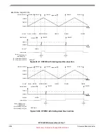
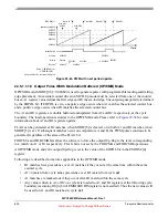
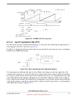
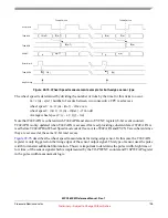
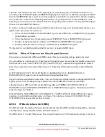
describes the operation of the OPWMB mode regarding A1 and B1 matches and the
transition of the channel output pin. In this example EDPOL is set to zero.
Figure 22-65. OPWMB Mode Matches and Flags
Note that the output pin transitions are based on the negedges of the A1 and B1 match signals.
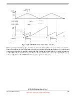
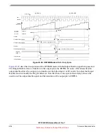
shows in cycle
n+1
the value of A1 register being set to zero. In this case the match posedge
is used instead of the negedge to transition the output flip-flop.
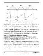
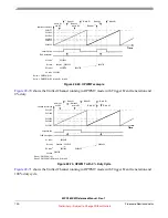
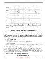
describes the channel operation for 0% duty cycle. Note that the A1 match posedge signal
occurs at the same time as the B1=$8 negedge signal. In this case A1 match has precedence over B1 match,
causing the output pin to remain at EDPOL bit value, thus generating a 0% duty cycle signal.
1
4
match A1 negedge detection
6
A1 value
$000004
A1 match
A1 match negedge detection
output pin
EDPOL = 0
TIME
match B1 negedge detection
B1 match
B1 match negedge detection
B1 value
$000006
clock
prescaler
A2 value
$000000
write to A2
$000000
A1 match posedge detection
match A1 posedge detection
1
cycle n
cycle n+1
8
6
FLAG set event
Selected
counter bus
FLAG pin/register


