


MPC563XM Reference Manual, Rev. 1
396
Freescale Semiconductor
Preliminary—Subject to Change Without Notice
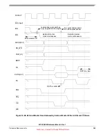
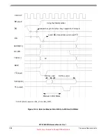
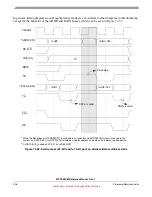
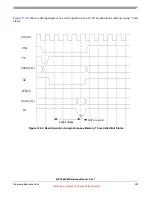
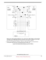
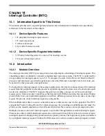
In general, timing diagrams in A/D multiplexing mode are very similar to other diagrams in this document,
except for the behavior of the ADDR and DATA busses, which can be seen in
Figure 13-52. Small access (32-bit read to 16-bit port) on Address/Data multiplexed bus
CLKOUT
*ADDR[3:31]
TS
**DATA[16:31]
TA
RD_WR
DATA is valid
TSIZ[0:1]
BDIP
OE
CSx
’10’
DATA is valid
Addr
Addr+0x2
Addr
Addr+0x2
Clock Gap
* While the EBI drives all of ADDR[3:31] to valid address, typically only ADDR[3:15] (or less) are used in the
system, as DATA[16:31] (or DATA[0:15]) would be used for address and data on an external muxed device.
** Or DATA[0:15], based on D16_31 bit in EBI_MCR.


