
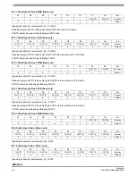


Sensors
Freescale Semiconductor
31
MMA7455L
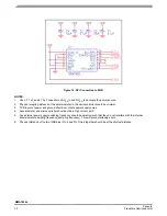
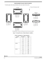
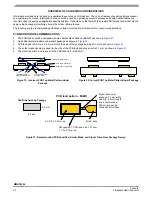
Figure 22. Stencil Design Guidelines
6.
Do not place any components or vias at a distance less than 2 mm from the package land area. This may cause additional
package stress if it is too close to the package land area.
7.
Signal traces connected to pads should be as symmetric as possible. Put dummy traces on NC pads in order to have same
length of exposed trace for all pads. Signal traces with 0.1 mm width and min. 0.5 mm length for all PCB land pads near the
package are recommended as shown in
and
. Wider trace can be continued after the 0.5 mm zone.
8.
Use a standard pick and place process and equipment. Do not us a hand soldering process.
9.
It is recommended to use a cleanable solder paste with an additional cleaning step after SMT mount.
10. Do not use a screw down or stacking to fix the PCB into an enclosure because this could bend the PCB putting stress on
the package.
11. The PCB should be rated for the multiple lead-free reflow condition with max 260°C temperature.
Please cross reference with the device data sheet for mounting guidelines specific to the exact device used.
Freescale LGA sensors are compliant with Restrictions on Hazardous Substances (RoHS), having halide free molding compound
(green) and lead-free terminations. These terminations are compatible with tin-lead (Sn-Pb) as well as tin-silver-copper
(Sn-Ag-Cu) solder paste soldering processes. Reflow profiles applicable to those processes can be used successfully for solder-
ing the devices.
14x0.575mm
Stencil opening = PCB landing
pad -0.025mm
= 0.575mmx0,875mm
Package
footprint
Signal trace near
package
10x0.8mm
14x0.875mm


