

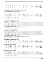


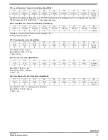


Sensors
30
Freescale Semiconductor
MMA7455L
OVERVIEW OF SOLDERING CONSIDERATIONS
Information provided here is based on experiments executed on LGA devices. They do not represent exact conditions present
at a customer site. Hence, information herein should be used as a guidance only and process and design optimizations are
recommended to develop an application specific solution. It should be noted that with the proper PCB footprint and solder stencil
designs the package will self-align during the solder reflow process.
The following are the recommended guidelines to follow for mounting LGA sensors for consumer applications.
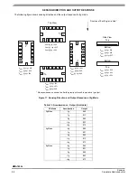
PCB MOUNTING RECOMMENDATIONS
1.
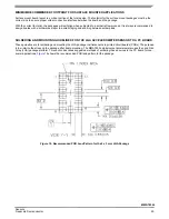
The PCB land should be designed with Non Solder Mask Defined (NSMD) as shown in
2.
No additional metal pattern underneath package as shown in
3.
PCB land pad is 0.9 mm x 0.6 mm which is the size of the package pad plus 0.1 mm as shown in
4.
The solder mask opening is equal to the size of the PCB land pad plus an extra 0.1 mm as shown in
.
5.
The stencil aperture size is equal to the PCB land pad – 0.025mm.
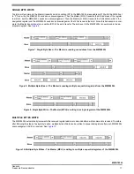
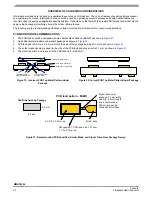
Figure 19. Incorrect PCB Top Metal Pattern Under
Package
Figure 20. Correct PCB Top Metal Pattern Under Package
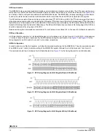
Figure 21. Recommended PCB Land Pad, Solder Mask, and Signal Trace Near Package Design
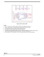
Example of 2 layer PCB
Top metal pattern
under package area
Via structure under
LGA package w/ solder
PCB top metal layer
Top metal pattern
under package area
Via structure under
package area
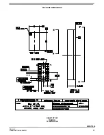
0.8 mm
0.5 mm
PCB land pattern - NSMD
SM opening = PCB land pad + 0.1mm
= 1.0 x 0.7mm sq.
Cu: 0.9 x 0.6 mm sq.
Signal trace near
package: 0.1mm width
and min. 0.5mm length
are recommended.
Wider trace can be
continued after these.
Wider trace
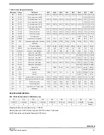
Pad Dimension by Package


