


Chapter 3 BIOS Description
33
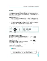
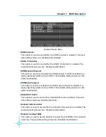
Advanced Chipset Features
v
DRAM Timing Selectable
This item determines DRAM clock/ timing using SPD or manual configuration.
The available setting values are: By SPD and Manual.
v
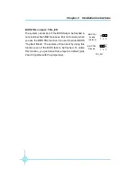
CAS Latency Time
This item determines CAS Latency. The available setting values are: 5, 4, 3
and Auto.
v
DRAM RAS# to CAS# Delay
This item allows you to select a delay time between the CAS and RAS strobe
signals. The available setting values are: 5, 4, 3, 2, and Auto.
v
DRAM RAS# Precharge
This item allows you to select the DRAM RAS# precharge time. The available
setting values are: 5, 4, 3, 2, and Auto.
v
Precharge delay(tRAS)
This item allows you to set the precharge delay time. The available setting
values are: Auto, 4 - 15.
v
SLP_S4# Assertion Width
This option indicates the assertion width of the SLP_S4# signal to guarantee
that the DRAMs have been safely power-cycled. The available setting values
are: 1 to 2 sec., 2 to 3 sec., 3 to 4 sec., 4 to 5 sec. .
v
System BIOS Cacheable
Select
“
Enabled
”
to allow caching of the system BIOS which may improve
performance. If any other program writes to this memory area, a system error
may result. The available setting values are: Enabled and Disabled.
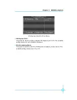
Advanced Chipset Features Menu


