


The connection to the USB has 16 data bits, 1 address bit, chip
select, wrn and rdn. An interrupt signal from the USB IC is
connected to the processor. See Figure 6-90 for a typical tim-
ing diagram. The USB IC is a complete USB unit. It is not
powered from the USB bus. The USB IC (U34) has a 6 MHz
oscillator. Check at C416.
The connection to the GPIB has 8 data bits, 5 address bits,
chip select, wrn, rdn and a special control signal for the level
shifting IC (U38). U38 is a buffer between the logic level of
+3.3 V for the processor and the logic level of +5 V for the
GPIB IC (U37). An interrupt signal from the GPIB IC is con-
nected to the processor. See Figure 6-91 for a typical timing
diagram. The GPIB IC is a complete GPIB unit. The GPIB IC
(U37) has a 40 MHz oscillator. Check at TP20.
Only the selected interface is involved in communication on
the microprocessor bus.
Since both interfaces consist of only one IC each, trouble-
shooting is fairly simple. Check that the oscillator (40 MHz or
6 MHz) is running. Check that the processor communicates
with the selected IC. Make sure the external controller (GPIB
or USB) and the interconnection cable used are OK.
The transfer of measurement results from the FPGA to the mi-
croprocessor goes via the 32-bit microprocessor bus and nor-
mal
reads
. There are some extra handshake pins to facilitate
the transfer. An interrupt signal is sent to the microprocessor if
results are to be read, ALERT, X30. X28 (EMPTY) indicates
that it is allowed to read results, and the microprocessor sets a
signal high to indicate that it is reading results, UPRD,
U11:203. Results are always read in packets of 8 words. See
Figure 6-92 for a typical timing diagram.
Another bus from the microprocessor is the SPI bus. It is a se-
rial bus with one data signal and one clock signal that are com-
mon to all ICs connected to the bus. A separate load signal for
each IC controls the loading of the data. Connected to the SPI
bus are (See Figure 6-93 to Figure 6-96):
•
The 100 MHz PLL IC (U9). The SPI bus is used only
for initialization after power on.
•
The optional oven oscillator IC (U5). The SPI bus is
used for initialization after power on and during a
timebase calibration.
•
The trigger levels IC (U46).
The last bus is the I
2
C bus. It is also a serial bus with two sig-
nals, SDA and SCL. Each connected IC has a unique address.
The message sent includes the address, and only the addressed
IC will listen to the message and respond by sending an ac-
knowledge to the master. Then it will react accordingly.
Introduction to the I
2
C Bus
The I
2
C bus is a 2-line serial bus for the communication be-
tween the ICs. The microprocessor controls the communica-
tion by means of the clock line SCL. One or more slaves can
read or write on the data line SDA.
The SDA and SCL are high at standby. All ICs connected to
the bus can sink SDA to low as they are interconnected via
open collector outputs. The microprocessor starts and stops
the communication by sending terms of start and stop:
During transmission the SDA can be changed only when the
SCL is low.
The microprocessor always begins to send the address infor-
mation. The format of this address information is seven ad-
dress bits, one read/write bit, and one acknowledge bit.
The addressed slave accepts by keeping the SDA line low
while the acknowledge bit (ACKN in ) is sent by the micro-
processor.
Example of addressing (address 30H):
The read/write bit R/W has the following meaning:
R/W = 1 means information from the slave to the µprocessor
R/W = 0 means information from the µprocessor to the slave.
The data information is sent after the address information.
The format of the data information is eight data bits followed
by one acknowledge bit. The reciever accepts by keeping the
SDA line low while the acknowledge bit (ACKN in ) is sent.
Example of data transmission (data 9BH):
6-50
Troubleshooting
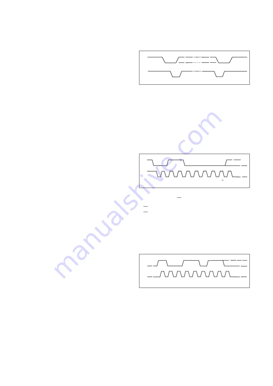
START
STOP
SDA
SCL
Figure 6-84
Terms of start and stop.
SDA
SCL
START
MSB
LSB
ACKN
R/W
1
2
3
4
5
1
6
1
7
8
9
Figure 6-85
Addressing.
SDA
SCL
MSB
LSB
ACKN
1
2
3
4
5
1
6
1
7
8
9
Figure 6-86
Data transmission.
Summary of Contents for PM6690
Page 1: ...Timer Counter Analyzer PM6690 Service Manual...
Page 4: ...This page is intentionally left blank IV...
Page 7: ...Chapter 1 Safety Instructions...
Page 11: ...Chapter 2 Performance Check...
Page 18: ...This page is intentionally left blank 2 8 Performance Check RF Options...
Page 19: ...Chapter 3 Disassembly...
Page 23: ...Chapter 4 Circuit Descriptions...
Page 24: ...This page is intentionally left blank 4 2...
Page 41: ...Chapter 5 Corrective Preventive Maintenance...
Page 44: ...This page is intentionally left blank 5 4 Other Important Information...
Page 45: ...Chapter 6 Repair...
Page 46: ...This page is intentionally left blank 6 2...
Page 104: ...This page is intentionally left blank 6 60 Safety Inspection and Test After Repair...
Page 105: ...Chapter 7 Calibration Adjustments...
Page 119: ...Chapter 8 Replacement Parts...
Page 147: ...Chapter 9 Schematic Diagrams...
Page 150: ...This page is intentionally left blank 9 4 Schematic Diagrams...
Page 151: ...This page is intentionally left blank Schematic Diagrams 9 5...
Page 152: ...Main Board PCB 1 Component Layout 9 6 Schematic Diagrams...
Page 154: ...9 8 Schematic Diagrams This page is intentionally left blank...
Page 156: ...9 10 Schematic Diagrams This page is intentionally left blank...
Page 158: ...9 12 Schematic Diagrams This page is intentionally left blank...
Page 160: ...9 14 Schematic Diagrams This page is intentionally left blank...
Page 162: ...9 16 Schematic Diagrams This page is intentionally left blank...
Page 164: ...9 18 Schematic Diagrams This page is intentionally left blank...
Page 166: ...This page is intentionally left blank 9 20 Schematic Diagrams...
Page 168: ...Display Keyboard PCB 2 Component Layout 9 22 Schematic Diagrams...
Page 170: ...This page is intentionally left blank 9 24 Schematic Diagrams...
Page 172: ...This page is intentionally left blank 9 26 Schematic Diagrams...
Page 173: ...Main Board PCB 1 Component Layout Bottom Side Schematic Diagrams 9 27...
Page 174: ...Main Board PCB 1 Component Layout Top Side 9 28 Schematic Diagrams...
Page 176: ...9 30 Schematic Diagrams This page is intentionally left blank...
Page 178: ...9 32 Schematic Diagrams This page is intentionally left blank...
Page 180: ...9 34 Schematic Diagrams This page is intentionally left blank...
Page 182: ...9 36 Schematic Diagrams This page is intentionally left blank...
Page 184: ...9 38 Schematic Diagrams This page is intentionally left blank...
Page 186: ...9 40 Schematic Diagrams This page is intentionally left blank...
Page 188: ...9 42 Schematic Diagrams This page is intentionally left blank...
Page 190: ...Display Keyboard PCB 2 Component Layout 9 44 Schematic Diagrams...
Page 192: ...9 46 Schematic Diagrams This page is intentionally left blank...
Page 193: ...Chapter 10 Appendix...
Page 196: ...This page is intentionally left blank 10 4 Glossary...
Page 197: ...Chapter 11 Index...
Page 200: ...This page is intentionally left blank 11 4 Index...