


Troubleshooting
6-41
must be replaced if the normal control voltage range cannot
make the oscillator output 10.000000 MHz.
As a last resort to exclude external causes of malfunction,
desolder the oven oscillator from the main circuit board.
Place it upside down and c12 V and ground accord-
ing to Figure 6-68. A cold oven oscillator draws approxi-
mately 0.30 - 0.35 A. During heating the current consumption
varies. After 10 minutes it should stabilize on less than 0.1 A.
The output V
ref
should be approxi5 V and the 10
MHz sinewave output signal should have an amplitude of
more than 2.5 V
pp
measured with a 1 M
W
, 10x probe. The
control input has an internal bias to keep the output frequency
in the middle of the range. Adjust the control voltage between
0 V and +5 V and check the output frequency range with a fre-
quency counter. The minimum trimming range should be
±5 Hz. 10.000000 MHz must be reached somewhere between
0 V and +5 V.
If the oven oscillator circuitry is repaired, a new calibration
must be performed. See Chapter 7. A new factory calibration
by means of the utility program should also be performed.
External Reference Input
See Figure 6-67 and Figure 6-70.
The input signal is amplified in U31. The output signal from
the amplifier should be a square wave with logic levels, repro-
ducing the timing characteristics of the input signal. Check
the signal at U32:11. U32 generates a short pulse (approxi-
mately 40 ns) for each input cycle, check at U32:9. These
pulses generate a broad spectrum of harmonics, and the
following high-Q 10 MHz crystal filter allows only a 10 MHz
sinewave to pass. Measure at X19. Note that the trimmer
C442 is used for maximizing the amplitude at X19. Check that
the amplitude is not less than 1 V
pp
. If external reference is not
selected, the gate U33 stops the 10 MHz signal. The control
signal on U33:1 is then low.
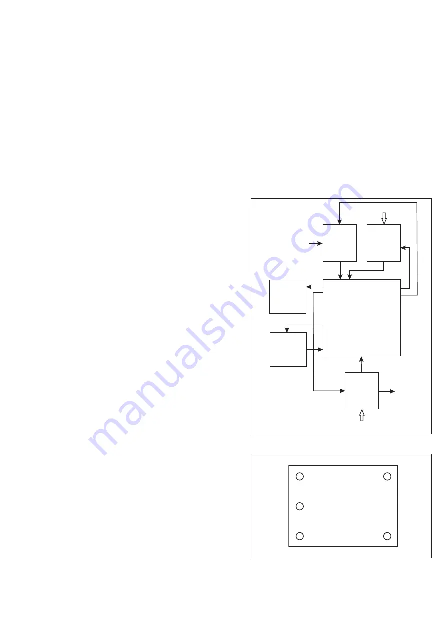
100 MHz Multiplier
See Figure 6-67 and Figure 6-69.
100 MHz is used in the measuring logic, mainly as a reference
clock, but also for other purposes. A PLL is used for multi-
plying the 10 MHz reference to 100 MHz. On power-up the
processor sets up the PLL IC (U9) via the SPI bus. An output
signal, PLL LOCK, tells the processor if the loop is locked
(high level). A VCO, consisting of an inverter (U47) and an
LC circuit in the feedback loop, is controlled by the PLL IC.
The DC voltage from U9:2 is filtered and controls a capaci-
tance diode. The VCO frequency changes with the capaci-
tance. The loop can handle the switching of 10 MHz refer-
ence, from internal to external and vice versa. There is no
need for a new setup. If external reference is selected and no
such signal is connected to the instrument, the PLL will be un-
FPGA
100 MHz
PLL
EXT REF
IN
INT REF
OUT
STD
OSC
OVEN
OSC
U4
U4-
U7
10 MHz
U11
ON/OFF
100 MHz
PLL
LOCK
(to
m
P)
ON/OFF
m
P/SPI
m
P
m
P/SPI
U41, Q53, Q54
U31, U32,
U33, Q55
U9, U47,
U48
Figure 6-67
Timebase reference system.
3
2
1
5
4
+12 V
Vref
Vcontrol
GND
10 MHz
OUT
Figure 6-68
Oven oscillator pinning (seen from bottom side).
Summary of Contents for PM6690
Page 1: ...Timer Counter Analyzer PM6690 Service Manual...
Page 4: ...This page is intentionally left blank IV...
Page 7: ...Chapter 1 Safety Instructions...
Page 11: ...Chapter 2 Performance Check...
Page 18: ...This page is intentionally left blank 2 8 Performance Check RF Options...
Page 19: ...Chapter 3 Disassembly...
Page 23: ...Chapter 4 Circuit Descriptions...
Page 24: ...This page is intentionally left blank 4 2...
Page 41: ...Chapter 5 Corrective Preventive Maintenance...
Page 44: ...This page is intentionally left blank 5 4 Other Important Information...
Page 45: ...Chapter 6 Repair...
Page 46: ...This page is intentionally left blank 6 2...
Page 104: ...This page is intentionally left blank 6 60 Safety Inspection and Test After Repair...
Page 105: ...Chapter 7 Calibration Adjustments...
Page 119: ...Chapter 8 Replacement Parts...
Page 147: ...Chapter 9 Schematic Diagrams...
Page 150: ...This page is intentionally left blank 9 4 Schematic Diagrams...
Page 151: ...This page is intentionally left blank Schematic Diagrams 9 5...
Page 152: ...Main Board PCB 1 Component Layout 9 6 Schematic Diagrams...
Page 154: ...9 8 Schematic Diagrams This page is intentionally left blank...
Page 156: ...9 10 Schematic Diagrams This page is intentionally left blank...
Page 158: ...9 12 Schematic Diagrams This page is intentionally left blank...
Page 160: ...9 14 Schematic Diagrams This page is intentionally left blank...
Page 162: ...9 16 Schematic Diagrams This page is intentionally left blank...
Page 164: ...9 18 Schematic Diagrams This page is intentionally left blank...
Page 166: ...This page is intentionally left blank 9 20 Schematic Diagrams...
Page 168: ...Display Keyboard PCB 2 Component Layout 9 22 Schematic Diagrams...
Page 170: ...This page is intentionally left blank 9 24 Schematic Diagrams...
Page 172: ...This page is intentionally left blank 9 26 Schematic Diagrams...
Page 173: ...Main Board PCB 1 Component Layout Bottom Side Schematic Diagrams 9 27...
Page 174: ...Main Board PCB 1 Component Layout Top Side 9 28 Schematic Diagrams...
Page 176: ...9 30 Schematic Diagrams This page is intentionally left blank...
Page 178: ...9 32 Schematic Diagrams This page is intentionally left blank...
Page 180: ...9 34 Schematic Diagrams This page is intentionally left blank...
Page 182: ...9 36 Schematic Diagrams This page is intentionally left blank...
Page 184: ...9 38 Schematic Diagrams This page is intentionally left blank...
Page 186: ...9 40 Schematic Diagrams This page is intentionally left blank...
Page 188: ...9 42 Schematic Diagrams This page is intentionally left blank...
Page 190: ...Display Keyboard PCB 2 Component Layout 9 44 Schematic Diagrams...
Page 192: ...9 46 Schematic Diagrams This page is intentionally left blank...
Page 193: ...Chapter 10 Appendix...
Page 196: ...This page is intentionally left blank 10 4 Glossary...
Page 197: ...Chapter 11 Index...
Page 200: ...This page is intentionally left blank 11 4 Index...